Graphene Biosensors

By , Founder, Cheap Tubes Inc.  ·  Last reviewed:

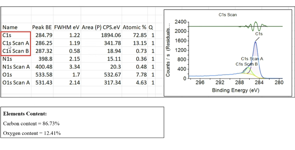
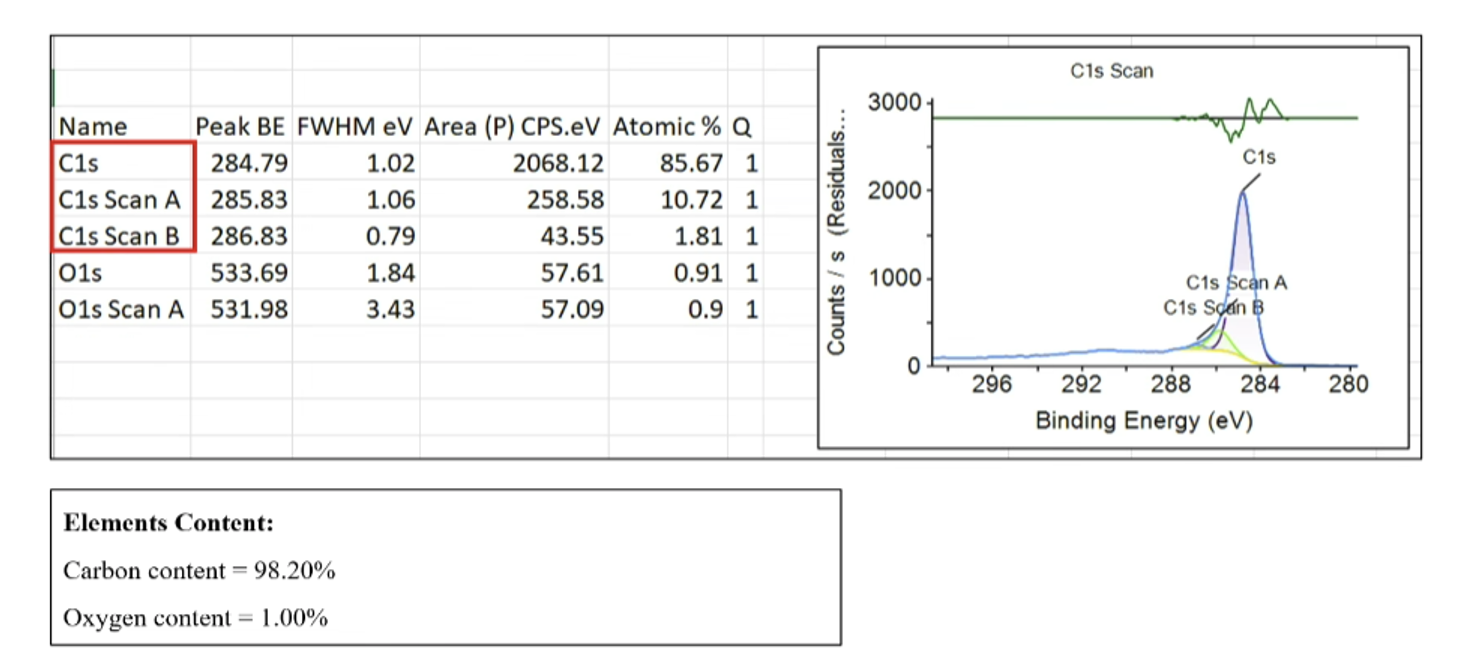
At a glance: Graphene-based biosensors leverage graphene’s high electrical conductivity, large surface-to-volume ratio, and biocompatible surface chemistry to detect biological analytes — glucose, proteins, DNA, pathogens — at very low concentrations. Common architectures include field-effect transistors (GFETs), electrochemical electrodes, and surface-plasmon-resonance devices. Performance depends on graphene purity, oxygen functional groups, and immobilization chemistry. Cheap Tubes supplies research-grade graphene, graphene oxide, and CVD graphene films suitable for biosensor prototyping.

Properties and Principles of Graphene Biosensors

Graphene’s mechanical, electrical and optical properties are the most useful for biosensing applications. It’s high mechanical strength, Young’s modulus, flexibility, and tensile strength are key properties during the fabrication process, as the surface is strong enough to be easily modified/be used to modify other surfaces. Efficient biosensors work by providing a high electron transfer rate between the electrode and the biomolecule. Graphene’s high charge mobility and electron transfer properties help to facilitate the electron movement between the target biomolecule and the sensor, making it a useful material in biosensing applications.

The doping ability and electrical conductivity of graphene makes it an ideal choice for mobilizing charge carriers in a sensor. When biomolecules are adsorbed onto a sheet of graphene, a change in the charge carrier density changes the electrical conductivity. The change in conductivity causes an electrical response that is measurable, which can be used to identify whether a molecule has been sensed or not.

Graphene is also transparent to visible-light wavelengths, making it useful in optical-based biosensors where the higher density of states of a biomolecule improves the surface electromagnetic wave propagation. Optical properties can be utilized in such situations where DNA bases wish to be identified, but not double stranded DNA. There are also four principles that are utilized when graphene used to sense biomolecules. These are: using graphene as electron transfer materials, electrochemical impedance materials, as field effect transistors (FETs) and as photon/phonon transfer materials.

Electron Transfer Materials Graphene is exploited as an electron transfer material because its high surface area can expose all of the carbon atoms to the target biomolecules, increasing the sensitivity (or it gives the potential for an increased sensitivity). The low noise also gives a higher sensitivity. Graphene can also be used as an electric transfer medium in sensors, where its high mobility and electrical conductivity help to facilitate the movement of charge and electron through the sensor.

Graphene is also able to act as an electron transport material by physically binding to the biomolecule and shifting electrons through bonding interactions. Impedance Materials To be used as an impedance material, graphene can be used to functionalise the electrode surface within a biosensor. Graphene’s delocalised π-network forms π-π stacking interactions which can anchor other π-conjugated molecules onto the electrode. This method provides a method to modify the surface of graphene in biosensors without disturbing its desirable electrical conductivity properties.

The high surface area of graphene provides many anchoring/binding sites for both target molecules and fabricated metal nanoparticles (which are sometimes used to improve the sensing efficiencies of biosensors). The aromatic domains on the graphene sheet (and ionic regions if metal nanoparticles are present) allow the graphene sensor to interact in various ways, which can increase the sensitivity against non-graphene biosensors.

FETs Using graphene as a suspended FET in FET-biosensors produces an enhancement in the sensitivity, owing to the interfacial charge traps which act as external scattering centres and degrade transport properties. Graphene is incorporated into two types of FET-based biosensors- back gate and liquid gate. In back gate FETs, the change in a threshold/source-drain voltage causes the conductivity of graphene to change, allowing for a higher sensitivity to be recorded.

In liquid gates FETs, graphene is very susceptible to a change in the surrounding liquid environment, whether it be by ion density or a surface charge, which produces a higher detection sensitivity compared to other non-graphene liquid gate FET biosensors. The surface of the graphene sheet can also be functionalised to be selective to a single biomolecule. The graphene sheet can detect electronic changes in the surrounding liquid medium by two different mechanisms- electrostatic gating mechanisms and surface transfer doping.

Electrostatic gating mechanisms exploit the hole density, which leads to a change in the overall conductivity of graphene causing a sensing response. Surface transfer doping is when a dopant/biomolecule induces a shift in the gate voltage of the graphene gate and causes a left shift of the Dirac point by a charge transfer mechanism, which represents a transfer of electrons from the biomolecule to the graphene gate. Such mechanisms invoke a response which can be detected and measured i.e. the electron transfer causes the molecule to be sensed.

Direct binding of biomolecules can also invoke a similar response, as the number of electron scattering centres becomes increased, resulting in a decrease in the mobility of graphene’s charge carriers. Photon/Phonon Transfer There are two main mechanisms that determine photon and phonon transfer through graphene. These are electrochemiluminescence (ECL) and fluorescence. ECL (without graphene) has two mechanisms; annihilation and co-reactant. Both mechanisms involve intermediate complexes undergoing an electron transfer reaction on the surface of the electrode.

Such mechanisms promote electrons into higher orbital states, where upon light is released when they return to their ground state. Graphene, however, produces two opposing mechanisms; ECL enhancement and ECL quenching. Graphene’s intrinsic electrical conductivity and mobility promote the quantum yield of the luminophore, which is normally limited by the electron transfer of a number of linked luminophores. Graphene’s efficient electrical properties promotes efficient electron transfer which induces a greater concentration of intermediate species to higher electronic states, per unit time.

This, coupled with graphene’s high surface area provides a high concentration of sites for both luminophores and target biomolecules, all of which increases the sensitivity of the sensor. Graphene (particularly GO) can also quench the ECL mechanism due to resonance energy transfer. There is a critical point for ECL intensity. Below this, the incorporation of graphene into the sensor increases the ECL intensity. Above this, the ECL intensity will decrease, even if graphene is continued to be added into the matrix.

This mechanism is not fully understood to date, but it is believed to be a product of the blackbody effect. Graphene also has the ability to fluoresce and quench fluorescence. Graphene can be used in sensors to detect the fluorescence imposed onto the graphene (or GO) sheet by photo-induced charge transfer and fluorescence resonance energy transfer mechanisms. Graphene (and GO) can also be used as an energy quencher for organic fluorophores and nanomaterials. The quenching mechanism for these types undergoes also undergoes a fluorescence resonance energy transfer mechanism.

Glucose Biosensors

With more than 30 different derivatives documented, graphene sensors that can detect glucose are a widely-established area. Depending on the type of sensor, sensitivities can range from 0.64-1100 µA mM-1 cm -2 and the linear range can vary between 0.05 µm and 32 mm. Many types of graphene electrode can be implemented into glucose sensors. Glucose sensors today contain many graphene derivatives that are composited with both biological and non-biological materials. The two main types of graphene electrodes employed in glucose sensors are enzymatic and non-enzymatic electrodes.

The most common glucose sensors are developed using enzymatic components and the sensing range for a glucose sensor generally lies between 1-60 mM. This is also the range for both diabetic and non-diabetic blood glucose levels. Whilst many variations of graphene can be utilised (including graphene nanosheets, nanoflowers, nanocubes, graphene ionic liquids, poly-functionalised graphene and graphene paper), pure graphene and reduced graphene oxide (rGO) are the most common graphene derivatives used in glucose sensing.

They form a wide range of composites with metal nanoparticles, polymers and conducting polymers, which are used to modify electrode surfaces. The sensing of glucose relies on two main factors- the efficient transfer of electrons between the glucose and the graphene and the presence of a catalytic material. The interaction of glucose and graphene produces well-defined redox peaks, which provides and efficient electron transfer system.

The redox potential between glucose and graphene is reversible, with a rate constant is 2.83 s-1, which is a much higher rate when compared to other carbon allotrope sensors, e.g. CNTs. Graphene also exhibits a high loading capacity of glucose onto its surface, due to its high surface area. Graphene glucose sensors almost always utilise metal nanoparticles on their surface due to their ability to enhance the sensitivity, electron transfer and response times.

An inexpensive, non-enzymatic, disposable sensor strip has been developed on the small scale, using a copper-graphene nanocomposite, to measure the glucose concentration in human tear fluids. The electrodes in these sensors contain surface modifications of copper nanoparticles, as the size and distribution of such nanoparticles play a big role in the optimization of the sensor. A larger copper concentration increase the output of the signal, due to an increased number of reactions between the copper ions and the glucose molecules.

The incorporation of graphene in the matrix creates a uniform distribution of copper NPs by controlling the electrodeposition under an applied voltage. By using oxygenated graphene (GO, rGO etc), the surface functional groups help to bind the copper nanoparticles in place, which helps to facilitate the exhibited uniform distribution. These glucose strips show a linear relationship between the current applied and the amount of glucose sensed, with an optimal working potential of 0.5 V.

These sensors have a sensitivity of 1101 µA mM-1 cm-2 with detection limits between 0.025 and 0.9 mM. These glucose strip sensors are also consistent, with a reproducibility of 91%. They also show a high stability. After 10 sensing cycles (with an applied current), over a 30-day period, the sensors have shown to exhibit a maximum loss of 17.2%. Enzyme-modified graphene solution-gated transistors can be used as high performance glucose sensors. These glucose sensors are a type of solution-gated graphene transistors (SGGTs).

SGGT’s have been found across various applications to provide, real-time, sensitive sensing with a high throughput. They can also operate in low voltages and aqueous environments, both of which are valuable properties for sensing biomolecules. The sensing mechanism of these sensors revolves around interactions between the biomolecules and the sensors channels/gates. The channels and gates in these glucose sensors are made of CVD graphene and the gate electrodes are modified with glucose oxidase (GOx) enzymes, biocompatible polymers and platinum nanoparticles.

The sensors work by oxidizing the glucose (GOx catalysed reaction) which generates hydrogen peroxide at the gates. The hydrogen peroxide is then oxidized, which regulates the effective gate voltage applied on the transistor. The sensors are sensitive to the voltage changes, which allows for a detection signal to be recorded. These sensors can show detection limits for glucose and hydrogen peroxide at 0.5 µM and 30 nM, respectively.

The high sensitivity of these sensors make them a great candidate for non-invasive glucose sensors, which detect glucose in human bodily fluids such as saliva. Other SGGTs which have been modified with glucose oxidase have also been recorded, with detection limits of 0.1-10.9 mM.

Other notable glucose sensors are those containing Nafion/GOx/multilayer film of ionic liquid–sulfonic acid-functionalized graphene, GOx/TiO2 NP-graphene/GCE and Pt nanoflowers/GO/GCE, which show sensitivities of 0.0718 nA µM-1, 6.2 µA mM-1 cm-2 and 0.64-1.26 µA mM-1 cm-2, respectively. 3-D graphene foam modified with cobalt oxide nanowires also show a very low detection limit of 25 nM. DNA Graphene can be used to distinguish individual nucleotide bases, single strand DNA and double strand DNA.

One of the simplest single strand DNA detection mechanisms is via immobilization of the DNA strand onto a functionalized graphene sheet (GO, rGO etc). Single strand DNA exhibits an orientation where all the nucleobases lie flat, which is favourable due to graphene’s planar/flat nature and high surface area. The bonding and hybridization between the amino-terminated groups of the DNA and the oxygen-based functional groups on the graphene sheet form amide bonds.

Using a graphene sheet with a higher concentration of carboxylic acid groups (i.e. rGO), improves the surface interaction between graphene and the DNA strand, due to the increased number of potential binding sites. Functionalized graphene can also bioconjugate with terminal sulphur groups on single strand DNA, although this is less common. The absorption of single strand DNA is very efficient, to the point where most of the bases become absorbed on to the graphene sheet and the helical structure can be destroyed.

Sensors based around various principles including fluorescence, electrochemical, electrical and SERS assays can be used for sensitive and selective double strand DNA recognition. Double strand DNA does not bind as strongly to graphene as single strand DNA does, due to a lower number of intermolecular interactions at the reactive interface. Single and double strand DNA can be differentiated by sensors using other non-conventional various methods with graphene as the binding material, including colorimetry, chemiluminescence and mass spectrometry.

Many sensing methods for the detection (and differentiation) of DNA using graphene revolve around π-π stacking interactions and other intermolecular forces. Graphene utilizes its exposed edge planes to catalyse and oxidise DNA bases better than any other electrode material. A sensor modified with graphene can exhibit up to a 4-fold greater sensitivity to DNA bases than other materials (including other carbon allotropes such as CNTs). Some reduced graphene oxide, dependent upon their functionalization, can detect and distinguish all four nucleotide bases and polymorphism in short oligonucleotides.

All the four bases exhibit different local density of states (LDOS) and interaction energies. The LDOS leave fingerprints specific to each base, which can be detected by local electron tunnelling conductance. The high conductivity of graphene allows for a higher detection sensitivity of these fingerprints. There are many different types of DNA sensor currently being researched, which incorporate the various mechanisms and principles discussed. One example is the utilization of graphene oxide and NaYF4:Yb,Er@SiO2 nanoparticles.

Like many DNA sensors, the driving mechanism is based around the π-π interactions between the carbon atoms (of the graphene) and the nucleobases (of the DNA). The interaction produces a fluorescence resonance energy transfer (FRET) quenching mechanism due to the overlap of the emission and absorption spectrums. These sensors have shown detection limits as low as 5 pM, with a selectivity for single stranded DNA. A graphene-FET based sensor has also been developed to detect mismatched DNA and polymorphisms.

These graphene sensors have a much simpler and cheaper fabrication compared to other polymorphism sensors. They also have a high specificity and the ability to detect a single nucleotide mismatch. The sensors measure a resistance induced by a displaced nucleotide strand, which induces a current change (of which graphene is highly sensitive to) and a shift in the Dirac point. The main advantage of these sensors is the ability to detect a single mismatch which is label-free and with high resolution.

These sensors are a very recent discovery which have the potential to form the basis for a commercial diagnostic point of care tool for early treatment of life-threatening diseases. Graphene quantum dots (GQDs) have also started to gain attention as DNA sensors. Double strand has a poor affinity to large sheet graphene, hence the preference to single strand selectivity. GQDs show a higher intercalation with DNA due to their smaller size.

The higher intercalation can promote DNA cleavage, so there is a future potential for GQDs to be a selective sensor for double strand DNA, once optimized. There are many different types of sensor for detecting various DNA forms. Other notable sensors include a ssDNA/azophloxine/graphene nanosheets sensor with a detection limit of 0.4 fM, a ssDNA/Au nanorods/GO/GCE sensor with a detection range of 0.035-3.5 fM and a ssDNA/GO–chitosan/ITO sensor with a detection limit of 10 fM.

Protein Biosensors

Another growing area with graphene based sensors is in the detection of proteins. Protein sensors are used to detect complex proteins such antibodies and biomarkers for use as diagnostic testing tools. Many protein sensors without graphene suffer from a lack of flexibility, making graphene a great material for composite protein sensors. A graphene nanoFET protein biosensor has been developed using CVD-grown graphene to detect thrombin biomarkers.

Unlike other graphene-based FETs for protein sensing (which generally use exfoliated graphene), the use of CVD-grown graphene allows for an easier scalability, easier fabrication procedure, larger sensing area and are reusable. They also provide similar advantages to other similar sensors such as low noise and high transconductance. The sensor is used to detect real-time binding (and unbinding) of thrombin protein biomarkers using the change in electrical current produced by the binding-unbinding mechanisms. These sensors are also able to measure the binding kinetics during the binding-unbinding processes.

These sensors have an effective gate voltage of 0.21 mV min-1, with a dissociation constant of 170 nM. The sensor can be regenerated with a simple rinse of buffer solution, which removes any bound protein on the surface. The surface of the sensor also contains a DNA aptamer which is specific for binding to thrombin. These DNA aptamers have a half-life of 10 hours i.e. 50% of the aptamer will have removed itself after 10 hours, but the device themselves have a shelf-life of over a week.

A protein sensor using thermally reduced graphene oxide (TRGO) and gold nanoparticles conjugated with antibodies. The sensor response, like many biosensors, occurs when a protein binds to the nanoparticle/antibody conjugates which induces a change in conductivity in the TRGO sheet. The signal is recorded by FET and direct current measurements. They are fabricated via many techniques including e-beam lithography, dispersion and suspension methods and multiple annealing steps. The AuNPs tested so far have been 10 and 20 nm in diameter, with 12 and 48 antibodies per each NP, respectively.

These sensors have a much higher sensitivity than many other carbon-based protein sensors, with a detection limit of 0.2 ng ml-1. This sensor has been developed off an unoptimized predecessor with an order of magnitude improved sensitivity, so the potential for these sensors may not have yet been reached, and the sensitivity could be further increased (although this has been stated by the researchers themselves that it would be a hard task).

A primitive bioelectronic sensor to detect proteins that fluoresce using a graphene FET with biological and inorganic functional groups has also been developed. The sensor works by detecting tagged proteins (e.g polyhistidine) which bind via the tag itself. The device provides an electric readout for each given protein by measuring the proteins optimal excitation wavelength. By knowing the excitation wavelength and making the surface multi-functional, they have the potential to be used as diagnostic tools in the future for the detection of various protein species.

The single protein detection devices to date adopt a p-type structure with a hole mobility’s between 300-2000 cm2 V s-1.

Other Small Biomolecule Biosensors

Aside from the main three biosensors described, other small biomolecules such as cells, electroactive analytes, dopamine and uric acid (to name a few) can now be detected by various graphene-based sensors. Graphene can be used as a biocompatible substrate to enhance the adhesion and growth of cells to detect cell populations. Graphene oxide with a negatively charged surface can be used to interact with positively charged poly-L-lysine, which results in a biocompatible interface that promotes cell adhesion for the detection of 30 cell mL-1.

A composite film of chemically rGO and carboxymethyl chitosan with folic acid molecules anchored to the surface can be used for the detection of tumour cells which have a folate receptor, at a rate of 500 cells mL-1. Another nanocomposite consisting of chemically rGO and 3,4,9,10-perylenetetracarboxylic acid can be used to detect breast and cervical carcinoma cells at a rate of 1000 cell mL-1.

These nanocomposites are deposited onto an electrode where the carboxylic acid groups are linked to a specific aptamer that binds to nucelolin (and overexpressed protein in the carcinoma cells). A common component of many small molecule sensors is either GCE or a graphite/GCE composite. However, many of these are being phased out and chemically reduced graphene oxide is being used to replace the graphite component, mainly due to its higher electron transfer rate.

The oxidation/reduction potentials to detect H2O2 (a common enzymatic byproduct) for GCE/Chemically rGO are 0.2/0.1 V compared to 0.8/-0.35 V and 0.7/-0.25 V for graphite/GCE and GCE, respectively. Chemically rGO also exhibits a wide linear range with values between 0.05-1500 µM than other sensors due to a higher concentration of edge plane defect. Chemically rGO electrodes also show great electron transfer rates for NADH at 0.4 V, which is 0.3 V lower than GCE/graphite sensor electrodes.

Chemically rGO electrodes show a great deal of promise in terms of linearity and limits of detection (LOD). For ascorbic acid, they show an LOD of 0.07 µM with a linearity of 0.1-106 µM. The electrodes can be heavily modified by a series of moieties, nanoparticles and inks to produce LOD’s that are wider ranging from 5 nM to 1.2 µM with linearity’s between 0.15-4500 µM. Chemically rGO/GCE electrodes shows a LOD of 0.12 µM and a linearity 0f 0.5-2000 µM for dopamine.

Functionalized chemically rGO/GCE electrodes show LOD’s as low as 22 nM with linearity’s ranging from 0.2-4000 µM. For uric acid, chemically rGO/GCE has a LOD of 0.2 µM with a linearity of 0.8-2500 µM. Modified electrodes can show an LOD of 0.088 µM with linearity’s of 0.1-1000 µM. In previous non-graphene sensors, the selectivity between dopamine, uric acid and ascorbic acid has always been poor as the sensors could not distinguish between these three molecules. These are also three of the most studied small biomolecules.

The sp2 planes and edge defects exhibited by graphene produces a greater number of π-π interactions that can be used to distinguish dopamine from other small biomolecules. There is still further work required to distinguish between other biomolecules, but using graphene instead of other carbon allotropes shows a step in the right direction for producing selective and sensitive small molecule biosensors.

Design of Experiments

Glucose Sensor There are many glucose sensors that can be fabricated, but here we focus on the SGGT sensor described above, as there is a great potential for this sensor to become more commercially available than other glucose sensors. To start, a series of solutions need to be prepared before fabrication. A CHIT polymer solution needs to made up (the rest can be used as purchased).

To make the solution, dissolve CHIT (0.5g) in an acetic solution (100 mL, 50 mM, pH 5-6) and electromagnetically stir overnight store in a refrigerator (4 °C). Prepare a GOx stock solution by dissolving in PBS and storing in a refrigerator (4 °C). Dilute a 5 %wt Nafion solution 10 times with isopropanol before use. To fabricate the device, deposit Au/Cr source and drain electrodes onto glass substrates by magneton sputtering, using a shadow mask. The Cr is used as an adhesion layer for the Au.

Grow single layer graphene by CVD on Cu foil (alternatively, this can be purchased) and transfer to the glass substrate with the Au electrodes. Pattern the graphene films by standard lithography to produce the graphene channel and gate. [In this case, the gate electrode was defined as 3 x 3 mm and the channel width and lengths were 0.2 and 3 mm, respectively]. Attach a PDMS wall to the substrate to enable the testing of the device in PBS solution.

Modify the graphene gate electrodes with Pt NPs by electrochemical deposition (5 mM H2PtCl6/0.1 M HCl aqueous solution). Apply a constant voltage (+0.2V, 120 s) to optimize the deposition. Rinse the graphene/Pt NPs with de-ionized water and use as the gate electrode. To prepare the GOx-CHIT/Nafion/PtNPs/graphene electrode, mix the GOx stock solution (50 µL) with the CHIT solution (0.5 %wt) and sonicate for 15 minutes. Take the graphene gate electrode and drop Nafion (10 µL, 0.5 %wt) onto the surface of the gate and dry at room temperature.

After that, drop coat the GOx-CHIT mixture (10 µL) onto the gate electrode and refrigerate overnight (4 °C) to dry the GOx-CHIT film. Wash the device with de-ionized water to remove unwanted residues and store in the refrigerator for future use. DNA Sensor Here we look at the novel sensor that has the potential for commercial use. As described above, it is a sensor that can detect mismatching of DNA to a single nucleobase mismatch, so it could have great importance once optimized.

To fabricate the sensor, place the graphene onto copper foil and spin coat PMMA onto the topside of the graphene sheet. Etch away the bottom of the graphene. PMMA acts as the supporting layer for the graphene sheet after etching the copper. Remove the back-side of the graphene by oxygen plasma etching and cut into pieces with scissors (tests done to date use 4 x 6 mm pieces). Etch the copper by floatation with ammonium persulfate (0.1 M, 5 hours) and rinse with deionized water overnight.

Transfer the PMMA supported graphene sheet onto a SiO2-coated silicon wafer, then remove the PMMA layer with acetone (60 °C, 1 hour). Anneal the sample under a hydrogen/argon atmosphere (300 °C, 2 hours). To fabricate the transistor, use silver paste as the conducting and drain electrodes at two ends of the graphene sheet. Use silicone rubber as the insulate for the source and drain electrodes. Protein Sensor Here is the detailed production step of a the nanoFET protein sensor, as described above.

The sensor shows a great promise for scalability and larger scale production, so it is a great example of a sensor that should be reproduced and optimized. To make the sensor, first, either grow or purchase CVD-grown grapehene (on Cu foil) and spin coat PMMA (2% solution of 495 Mw PMMA in anisole) onto a square piece of graphene (1.5 x 1.5 cm).

Place the coated graphene square into a copper etchant (4 hours) and then clean the device by soaking it in deionized water baths for at least 12 hours and transfer onto the device substrate (Si/SiO2 with 500 nm oxide and pre-defined alignment marks). Dry the device (30 °C, 4 hours) and remove the excess PMMA by open-air heating (350°C, 4 hours). Pattern graphene ribbons (3 µm x 10 µm) using photolithography and an O2 plasma etcher.

After patterning, fabricate metal electrodes (1.5 nm Cr/30 nm Au) using standard lithography, metallization and lift-off methods. This leaves an exposed graphene area of 3 x 3 µm and is the active sensing area (24 in total over the device). Remove the residues by annealing the device (400 °C, Ar/H2 atmosphere). To make the surface preferential for protein binding, treat the device with pyrenebutanoic acid succinimidyl ester (PBASE) and a thrombin-specific DNA-based aptamer.

Future Advancements

Many graphene-based biosensors have only been tested on the small/laboratory scale. The next big step, like many graphene composite materials, is to optimize their sensitivity and selectivity to push production to commercial levels. For sensors that are looking to analyse in-vivo, discovering the toxicological and biocompatibility effects of graphene will decide if the sensors are to be used in this capacity. Many graphene biosensors exhibit similar sensitivities to other non-graphene biosensors, but can exhibit beneficial properties such as enhanced flexibility, conductivity and selectivity to certain molecules.

To take these sensors to the next level in terms of production, an increase in the sensitivity to greater levels (to confidently surpass existing sensors) is needed, as is the ability to be able to select and distinguish between various biomolecules. The ability to do the latter will push graphene-based biosensors to significant heights above their non-graphene counterparts. This should be the focus and it is the property that will offer the most benefit for commercial applications e.g. as multi-functional diagnostic tools.

References

Kumar S., Luong J.H.T., Recent advances in electrochemical biosensing schemes using graphene and graphene-based nanocomposites, Carbon, 2014, 84(1), 519-550 Tehrani F., Reiner L., Bavarian B., Rapid prototyping of a high sensitivity graphene based glucose sensor strip, PLoS ONE, 2015, 10(12), 1-11 Wang F., Liu L., Li W., Graphene-based glucose sensors: A brief review, IEEE Transactions on Nanobioscience, 2015, 14(8), 818-834 Zhang M., Liao C., Mak C.H., You P., Mak C.L., Yan F., Highly sensitive glucose sensors based on enzyme-modified whole-graphene solution-gated transistors, Scientific Reports, 2015, 5:8311, 1-6 Hu Y., Li F., Han D., Niu L., Biocompatible graphene for bioanalytical applications, Springer, 2015, VIII, Chapter 2, pages 11-33.

Alonso-Cristobal P., Vilela P., El-Sagheer A., Lopez-Cabarcos E., Brown T., Muskens O. L., Rubio-Retama J., Kanaras A. G., Highly sensitive DNA sensor based on upconversion nanoparticles and graphene oxide, ACS Appl. Mater. Interfaces, 2015, 7, 12422−12429 Hwang M. T., Landon B. P., Lee J., Choi D., Mo A. H., Glinsky G., Lal R., Highly specific SNP detection using 2D graphene electronics and DNA strand displacement, PNAS, 2016, 113(26), 7088-7093 Saltzgaber G., Wojcik P., Sharf T., Leyden M. R., Wardini J. L., Heist C. A., Adenuga A. A., Remcho V.

T., Minot E. D., Scalable graphene field-effect sensors for specific protein detection, Nanotechnology, 2013, 24, 355502 Mao S., Yu K., Lu G., Chen J., Highly sensitive protein sensor based on thermally-reduced graphene oxide field-effect transistor, Nano Res., 2011, 4(10), 921-930 Lu Y., Lerner M. B., Qi Z. J., Mitala Jr. J. J., Lim J. H., Discher B. M., Johnson A. T. C., Graphene-protein bioelectronic devices with wavelength-dependent photoresponse, Applied Physics Letters, 2012, 100, 033110

Graphene Materials for Biosensor Research

We supply graphene oxide, reduced graphene oxide, and graphene nanoplatelets optimized for biosensor electrode fabrication — including CVD graphene films for FET-based detection. Technical specs, SDS, and bulk pricing on request.

Shop Graphene Oxide →Shop Graphene Nanoplatelets →


About the author

Mike Foley is the founder of Cheap Tubes Inc., a Vermont-based supplier of research-grade carbon nanomaterials since 2005.

He has a BS in Business Administration and a high-tech manufacturing background spanning wafer fabs, thin-film optics, and nanotechnology, with a pending patent application related to nanoparticle dispersion. Cheap Tubes supplies carbon nanotubes, graphene, graphene oxide, MXene, and specialty nanomaterials to researchers and engineers in 50+ countries.

More about Cheap Tubes  ·  Contact / Request a quote  ·  All resources

Graphene Oxide Buying Guide: How to Choose the Right Form, Layer Count, and Flake Size

By , Founder, Cheap Tubes Inc.  ·  Last reviewed:

TL;DR: Choosing graphene oxide comes down to three decisions: form (oxide, reduced, or exfoliated), layer count (single layer, 2–4 layer, or multilayer), and flake size (450 nm to 50+ µm). For lithium-ion battery electrodes, choose Reduced Graphene Oxide Industrial Grade ($110/g) or Exfoliated rGO Powder ($115/g). For polymer composites and bulk research, Graphene Oxide Powder at $90/g is the industrial-grade choice. For sensors, membranes, and biomedical work where defect-free single sheets matter, Single Layer Graphene Oxide at $140/g or the size-controlled 450 nm and 1-20 µm variants are the right call. Every Cheap Tubes order ships with a Technical Data Sheet (TDS) and Safety Data Sheet (SDS).

By Mike Foley, Founder, Cheap Tubes Inc. — published April 2026

Graphene Oxide vs Reduced Graphene Oxide Graphene Oxide (GO) OH O COOH Oxygen functional groups: hydrophilic, insulating, reactive Reduction Ar / H₂ 200–400 °C Reduced Graphene Oxide (rGO) Restored sp² conjugation: conductive, hydrophobic

1. The Three Decisions That Determine Which GO You Need

Graphene oxide is not a single material. It’s a family of related carbon nanomaterials, each with measurably different chemistry, conductivity, surface area, and dispersion behavior. The “right” graphene oxide for your work depends entirely on three questions:

  1. Do you need oxygen functional groups, or do you need conductivity? This determines whether you want graphene oxide (GO), reduced graphene oxide (rGO), or exfoliated rGO. They look similar in a vial but behave very differently in your experiment.
  2. Does your application need single sheets, or are stacks acceptable? This is your layer count decision. Single-layer (1L) is most expensive and offers maximum surface area; few-layer (2-4L) is a practical compromise; multi-layer / standard powder is most cost-effective.
  3. Does flake size matter for your process? Smaller flakes (450 nm) disperse better in inks and biomedical formulations. Larger flakes (1-20 µm) provide more continuous conductive paths for sensors and films.

Get those three right, and you’re in a narrow set of products that will work for your application.

2. Quick Comparison: All 8 GO Products at a Glance

# Product Form Layers Flake size Price (volume) Best for
1 Graphene Oxide Powder Oxide Multilayer Standard (300-800 nm) from $90/g Bulk research, polymer composites, industrial-grade
2 Reduced Graphene Oxide Industrial Grade Reduced Multilayer Standard from $110/g Battery electrodes, conductive composites at scale
3 Exfoliated Reduced Graphene Oxide Powder Exfoliated Few-layer Standard from $115/g High-conductivity composites, supercapacitors
4 Single Layer Graphene Oxide Oxide 1L 300-800 nm from $140/g Sensors, membranes, baseline single-sheet research
5 Few Layer Graphene Oxide 2-4L Oxide 2–4L Standard from $140/g Performance/cost compromise, electrochemistry
6 Reduced Graphene Oxide Reduced Multilayer Standard from $190/g Sensitive electrochemistry, higher-purity rGO
7 Single Layer GO 1-20 µm Oxide 1L 1-20 µm (premium size) from $190/g Large-flake sensors, transparent conductive films
8 Single Layer GO 450 nm Oxide 1L <450 nm (premium size) from $190/g Inks, biomedical, drug delivery

Specialty: Graphene Oxide Gel is available as a pre-dispersed format on request — most graphene oxide disperses readily in water with brief sonication, so the gel is a niche convenience format rather than a primary recommendation.

Pricing note: Pricing varies by quantity. Established products (Single Layer GO, Few Layer GO, the size variants, and the premium Reduced Graphene Oxide) show volume-tier pricing for 10 g+ orders. Newer products (Graphene Oxide Powder, rGO Industrial Grade, Exfoliated rGO Powder) currently show single-gram pricing — volume tiers will be added as demand stabilizes. Size-controlled variants (450 nm and 1-20 µm) command a premium over the standard 300-800 nm flake size. Refer to each product page for current quantity-tier pricing.

All products ship from Vermont with a Technical Data Sheet (TDS) and Safety Data Sheet (SDS). Bulk pricing is available — contact us for orders above 100 g.

XRD pattern of Cheap Tubes Graphene Oxide Powder (SKU 060106) showing the (001) diffraction peak at ~11° 2θ
XRD pattern of Graphene Oxide Powder (SKU 060106) — the strong, sharp (001) reflection at 2θ ≈ 11° corresponds to expanded interlayer spacing from intercalated oxygen functional groups, the signature of well-oxidized, layered GO. The broad reflection near 42°–44° corresponds to the in-plane (100) carbon lattice.

3. Decision Tree by Application

Find your application below. Each section names the product we recommend and explains why.

3.1 Lithium-ion Battery Electrodes (Anode or Cathode Conductive Additive)

Primary: Reduced Graphene Oxide Industrial Grade — from $110/g
Alternative: Exfoliated Reduced Graphene Oxide Powder — from $115/g

Why rGO and not GO: Battery applications demand electrical conductivity, not surface chemistry. Graphene oxide’s oxygen functional groups (hydroxyl, epoxy, carboxyl) interrupt the conjugated π-system that carries current. Chemical or thermal reduction strips those groups, restoring conductivity to within ~1-2 orders of magnitude of pristine graphene. For Li-ion electrodes, this matters: rGO can replace or supplement carbon black as a conductive additive at lower loading, improving rate capability without dramatically increasing inactive mass.

Industrial Grade vs Exfoliated: Industrial Grade rGO is multilayer and most cost-effective at scale (kilogram quantities for prototype cell builds). Exfoliated rGO has been mechanically separated into thinner stacks during processing, giving higher specific surface area and more accessible electrochemical sites — useful for higher-performance cells where capacity retention at high C-rate is the bottleneck. Both ship with conductivity data on the TDS.

For sensitive electrochemistry where trace metallic impurities from chemical reduction would interfere (e.g., pristine cathode work, metal-air batteries), our premium Reduced Graphene Oxide at $190/g is purified to a higher standard.

Reduced graphene oxide as conductive additive in lithium-ion battery
Reduced graphene oxide as a conductive additive in lithium-ion battery electrodes — rGO sheets connect active particles into a percolating conductive network without adding significant inactive mass.

3.2 Polymer Composites (Mechanical Reinforcement, Conductive Plastics)

Primary: Graphene Oxide Powder — from $90/g for nonconductive reinforcement
For conductive composites: Exfoliated rGO Powder — from $115/g

Why GO for mechanical work: Graphene oxide’s surface oxygen groups make it covalently or hydrogen-bond compatible with most polar polymer matrices — epoxy, polyamide, PVA, polyurethane. Single-sheet dispersion isn’t required for tensile-modulus improvement; multilayer GO at 0.5-2 wt% loading achieves measurable property gains in well-mixed composites. Use GO Powder when your matrix is a thermoset epoxy or polar thermoplastic.

Why exfoliated rGO for conductive composites: When you need both mechanical reinforcement and electrical percolation (e.g., antistatic plastics, EMI shielding compounds), rGO is the single-component answer. Exfoliated rGO provides higher aspect ratio per gram than the standard industrial grade, lowering the percolation threshold.

3.3 Inks, Coatings, and Spray Formulations

Primary: Single Layer Graphene Oxide 450 nm — from $190/g

Why size-controlled small flakes: Inks and coatings require uniform dispersion that doesn’t settle, clog spray nozzles, or produce visible defects in dried films. Sub-micron flake size (450 nm median) eliminates the gross sedimentation problems associated with multi-micron flakes, while the high oxygen content of single-layer GO keeps dispersions stable in water and polar organic solvents (DMF, NMP, DMSO) without surfactants.

If your application is a transparent conductive coating (where transparency depends on flake-size uniformity and rGO is required for conductivity), the workflow is: disperse 450 nm GO, deposit, then thermally or chemically reduce on the substrate.

3.4 Sensors, Biosensors, and Field-Effect Devices

Primary: Single Layer GO 1-20 µm — from $190/g

Why large single sheets: Sensor performance depends on the continuous conductive path across the active area. Multi-flake interfaces introduce contact resistance and noise. Single-sheet 1-20 µm flakes can span practical sensor channel dimensions (typically 1-10 µm) with a single piece of material, eliminating those contact problems.

For chemical sensors where surface oxygen groups are the sensing chemistry, use the as-supplied GO. For FET-style devices where conductivity matters, reduce the GO post-deposition (vapor-phase hydrazine, thermal anneal at 200-300 °C in inert atmosphere, or photochemical reduction).

3.5 Membranes (Water Filtration, Gas Separation)

Primary: Single Layer Graphene Oxide — from $140/g or Single Layer GO 1-20 µm — from $190/g for thicker/larger-area membranes

Why single-layer GO: Membrane separation depends on the controlled inter-sheet spacing of stacked GO sheets — typically 0.7-1.4 nm depending on hydration. Single-layer feedstock produces the most predictable interlayer chemistry; multilayer feedstock dilutes the active surface and introduces flake-edge defects that act as bypass channels.

For lab-scale membrane research at typical sample sizes (a few cm²), the standard Single Layer GO is the cost-effective starting point. For larger membranes or applications where consistent flake size matters more than interlayer chemistry, the 1-20 µm size-controlled variant gives more reproducible casting.

3.6 Biomedical (Drug Delivery, Bioimaging, Antibacterial Coatings)

Primary: Single Layer GO 450 nm — from $190/g

Why small single-layer flakes: Biomedical applications demand cellular-scale dimensions (sub-micron) for cell uptake or tissue penetration, single-layer chemistry for predictable surface functionalization (PEGylation, antibody conjugation, drug loading via π-π stacking), and tight size control to satisfy regulatory characterization. The 450 nm variant has been size-fractionated specifically for these applications.

GO is preferred over rGO for biomedical work — the oxygen functional groups are essential for both colloidal stability in physiological buffers and for the conjugation chemistry that attaches targeting moieties or therapeutic payloads.

3.7 Industrial-Grade Polymer and Bulk Applications

Primary: Graphene Oxide Powder — from $90/g

This is the industrial-grade choice for applications where multilayer graphene oxide is acceptable and larger flakes are actually beneficial — most polymer composite work falls here. Larger, multilayer flakes integrate well into polymer matrices, contribute meaningfully to mechanical properties at modest loading, and don’t carry the cost of single-layer or size-controlled variants. Use this product for thermosetting epoxies, polyamide composites, polyurethane reinforcement, screening studies, and any process where you’re optimizing matrix dispersion rather than chasing single-sheet performance. Bulk discounts apply at 50 g+; contact us for kilogram pricing.

4. GO vs rGO: When You Need to Reduce

Graphene oxide and reduced graphene oxide are produced from the same precursor (typically graphite via Hummers-method oxidation, then exfoliation), but the reduction step transforms the material’s chemistry, electrical properties, and dispersibility. Picking the wrong one is the single most common buyer mistake.

Graphene oxide (GO):

  • Carbon-to-oxygen ratio typically 2:1
  • Hydroxyl, epoxy, carboxyl groups on basal plane and edges
  • Insulating (sheet resistance 10⁹–10¹² Ω/sq)
  • Disperses readily in water (1-5 mg/mL) and polar organics
  • Hydrophilic — colloidal stability without surfactants
  • Compatible with conjugation chemistry (EDC/NHS coupling, click chemistry)

Reduced graphene oxide (rGO):

  • Carbon-to-oxygen ratio typically 8:1 to 12:1 (after thermal/chemical reduction)
  • Most oxygen groups removed; π-conjugation partially restored
  • Conductive (sheet resistance 10²–10⁵ Ω/sq depending on reduction)
  • Hydrophobic; dispersion in water requires surfactants or sonication
  • Mechanical and thermal properties closer to pristine graphene

Which GO do I need? If your application uses electricity (current, capacitance, sensing impedance), choose rGO. If your application uses chemistry (functional groups, hydrogen bonding, biomolecule conjugation, hydrophilic dispersion), choose GO.

Mid-cases — when GO + post-reduction is the right choice: If you need GO’s processability (water dispersion for casting, spray, or printing) but conductivity in the final product, the workflow is: disperse GO, deposit, then reduce in place. We’ve supplied this combination to many electrode-manufacturing labs.

Practical thermal reduction protocol: Once a GO film is deposited, you can achieve good reduction by heating the dried film in an inert atmosphere — typically argon with a small fraction of hydrogen — at 200–400 °C. This converts most of the residual oxygen functionality back to sp² carbon and recovers a substantial fraction of the conductivity of pristine graphene, without requiring chemical reductants or specialized equipment. Higher temperatures (toward 400 °C) give more complete reduction but require thermally stable substrates. Hydrazine vapor treatment is the more reactive alternative for thermally sensitive substrates; it works at near-room temperature but requires careful safety handling and waste disposal.

5. Layer Count: Single Layer vs Few Layer vs Multilayer

The “graphene” in graphene oxide can mean a single sheet or a stack of several sheets. The difference matters for any application where the oxygen-functional-group density per gram, surface area, or interlayer spacing controls performance.

Single Layer (1L):

  • Highest specific surface area (>700 m²/g for ideal 1L)
  • Maximum oxygen-group density per gram
  • Most expensive (more processing steps to delaminate)
  • Best for: membranes, sensors, biomedical, precision electrochemistry

Few Layer (2-4L):

  • Surface area ~200-400 m²/g
  • Performance/cost compromise — most physical-property advantages of 1L at lower cost
  • Most consistent batch-to-batch (less dependent on exfoliation completeness)
  • Best for: composites, electrochemistry, general research

Multilayer (Standard Powder):

  • Bulk material; layer count varies (typically 5-20 layers)
  • Most cost-effective per gram
  • Sufficient for many polymer-composite and electrochemistry applications
  • Best for: bulk research, cost-sensitive work, formulation development

Practical guide: Prototyping and academic research typically use single-layer GO so the reported results aren’t confounded by layer-count variability. Multilayer is the right choice for commercial applications — polymer composites, conductive masterbatches, and any process where consistent industrial-grade performance at lower cost is the goal.

XRD pattern of Cheap Tubes Exfoliated Reduced Graphene Oxide Powder (SKU 060108) showing loss of the GO (001) peak
XRD pattern of Exfoliated Reduced Graphene Oxide Powder (SKU 060108). The disappearance of the sharp GO (001) reflection at ~11° 2θ, combined with a broad amorphous hump near 20°–30°, indicates exfoliation and loss of long-range layered ordering — consistent with successful reduction and few-layer rGO.

6. Flake Size Selection

Lateral flake size affects how the material processes, disperses, and performs in your final composite or device.

450 nm (small):

  • Excellent dispersion stability (slower sedimentation by Stokes’ law)
  • Compatible with spray coating, inkjet printing, biological systems
  • Lower contact-resistance benefit at sensor scale (more inter-flake junctions)

1-20 µm (medium-large):

  • Better continuous conductive paths in films
  • Practical for transparent electrodes, EMI films, larger membrane areas
  • Some sedimentation in thin (<1 wt%) dispersions over hours-to-days

Standard / unspecified (~50+ µm typical for bulk powder):

  • Most cost-effective
  • Acceptable for composites, bulk electrochemistry, general research
  • May need size-fractionation for specific applications

If you’re not sure which size, start with the standard Single Layer GO or the bulk Powder and characterize what you actually have via dynamic light scattering or AFM before committing to a size-specific variant.

AFM image of Single Layer Graphene Oxide at sub-450 nm flake size
AFM image of Single Layer Graphene Oxide at <450 nm flake size (SKU 060101). Sub-micron lateral dimensions and ~1 nm sheet thickness suit ink, biomedical, and high-stability dispersion applications.
AFM image of Single Layer Graphene Oxide at 300-800 nm flake size
AFM image of standard Single Layer Graphene Oxide at 300-800 nm flake size (SKU 060102). The size distribution shown here is the baseline against which the 450 nm and 1-20 µm variants are size-fractionated.

7. What Ships With Every Cheap Tubes Order

Every order ships with two documents:

  • Technical Data Sheet (TDS) — specifications, characterization summary (XPS, Raman, BET surface area, particle size where relevant), and recommended handling.
  • Safety Data Sheet (SDS) — GHS-compliant safety, transport, storage, and disposal information. View all SDS documents.

Cheap Tubes Inc was founded in 2005 in Townshend, Vermont. We’ve supplied research-grade nanomaterials — carbon nanotubes, graphene, fullerenes, MXene, and graphene oxide — to over 10,000 customers across academia, industry, and government for 21 years. Published specs, real characterization, and shipped paperwork are not features. They’re our minimum.

Need bulk pricing, custom specifications, or a TDS sample before ordering? Contact us.

8. Frequently Asked Questions

What’s the difference between graphene oxide and reduced graphene oxide?
Graphene oxide retains the oxygen functional groups (hydroxyl, epoxy, carboxyl) that make it hydrophilic, easy to disperse in water, and chemically reactive — but those same groups make it electrically insulating. Reduced graphene oxide has had most of those oxygen groups removed (chemically, thermally, or electrochemically), restoring electrical conductivity at the cost of dispersibility. Use GO for chemistry; use rGO for electricity.

How do I reduce graphene oxide myself?
Two practical methods cover most lab needs:

  • Thermal reduction in inert atmosphere — once a GO film or coating is dried on the substrate, anneal it at 200–400 °C in argon (typically with a small fraction of hydrogen, e.g., Ar/H₂ 95/5). This is the protocol we use ourselves and recommend for substrates that tolerate the temperature. Reduction extent scales with temperature and dwell time — 30–60 minutes at 250–300 °C is a reasonable starting point for thin films; higher temperatures or longer holds increase the C/O ratio further. The atmosphere prevents oxidation; the optional H₂ accelerates removal of oxygen functional groups.
  • Hydrazine vapor treatment — for thermally sensitive substrates (polymers, biological surfaces), expose the GO film to hydrazine vapor at 60–100 °C for several hours. This works at lower temperatures but requires fume hood, careful waste disposal, and PPE. Hydrazine is acutely toxic and a suspected carcinogen.

For dispersions or bulk powder reduction, chemical reductants (sodium borohydride, ascorbic acid, hydrazine in solution) are options but typically leave more residual functional groups than thermal annealing. If you need pre-reduced material, our Reduced Graphene Oxide Industrial Grade and Exfoliated rGO Powder ship already reduced with characterization data on the TDS.

How do I disperse graphene oxide?
Most graphene oxide products disperse readily in water at 1-5 mg/mL. A bath sonicator works for screening and casual dispersions, but for reproducible, high-quality dispersions we recommend a probe-style (tip) sonicator — it delivers far higher localized energy and produces more uniform sheet exfoliation. Typical conditions: 5–15 minutes at 30–50% amplitude with the probe submerged in a small volume (10–50 mL) and the vessel ice-bathed to prevent heating. Single-layer GO disperses faster and at higher concentrations than multilayer. Polar organic solvents (DMF, NMP, DMSO, ethanol) also work; non-polar solvents (toluene, hexane) do not. Reduced GO is hydrophobic and typically requires either surfactants or solvent exchange — refer to the TDS for recommended dispersion conditions for your specific lot.

Does graphene oxide ship hazmat?
GO and rGO powders ship as ground-non-hazardous (UN classification N.O.S. when in non-fibrous powder form below regulatory thresholds). Air shipment is possible but check our SDS for the latest classification. International shipments may have country-specific restrictions; contact us before placing an international order.

What’s the shelf life of GO and rGO powders?
Refrigerated storage is recommended to preserve GO solubility — over time, GO powder stored at room temperature can lose dispersibility as oxygen functional groups slowly migrate or rearrange, reducing the easy water-dispersion behavior that makes GO useful. Stored sealed in a refrigerator: GO powder maintains its as-supplied solubility and oxygen content for 18-24 months. rGO is more stable (less reactive) and tolerates room-temperature storage; typically 36+ months sealed. Sonicated dispersions in water are stable for 4-8 weeks if refrigerated and protected from light; we recommend preparing dispersions fresh for critical experiments.

Can I get bulk pricing?
Yes. Quantities above 50 g typically receive a tiered discount; orders of 1 kg or more are quoted individually based on layer-count and characterization requirements. Contact us with your target quantity and application — we’ll match you with the right product and quote within one business day.

Do you sell custom particle sizes?
We carry the size variants listed in this guide (450 nm, 1-20 µm, and standard bulk). Custom size fractionation is available on a project basis for orders above 50 g — contact us with your target size distribution and we’ll quote process and lead time.

How do I store unused product?
Keep powders sealed in the original container, away from direct light, humidity, and oxidizing atmospheres. Refrigeration is recommended for GO powders to preserve solubility; rGO tolerates room-temperature storage. For dispersions: refrigerate (2-8 °C), shield from light, and re-sonicate briefly before re-use to redisperse any sediment.

What’s the difference between Single Layer GO 450 nm (SKU 060101) and Single Layer GO 1-20 µm (SKU 060103)?
Both are single-layer graphene oxide with the same oxygen-content range, produced from the same precursor. The difference is post-exfoliation size fractionation: 060101 has been processed to a 450 nm median lateral dimension; 060103 has been processed to a 1-20 µm size range. Choose 060101 for biomedical, ink, and high-stability dispersion applications; choose 060103 for sensor channels, transparent conductive films, and large-area membranes.

9. Related Resources and Products

If you came here researching graphene oxide but want broader context:

Browse the full GO product line: Graphene Oxide category

Other nanomaterials at Cheap Tubes: Graphene Nanoplatelets | Carbon Nanotubes | Fullerenes | MXene

Last reviewed: April 2026. Specifications and pricing on this page are current as of publication; refer to individual product pages for the most up-to-date specifications and any inventory-related notes.


About the author

Mike Foley is the founder of Cheap Tubes Inc., a Vermont-based supplier of research-grade carbon nanomaterials since 2005.

He has a BS in Business Administration and a high-tech manufacturing background spanning wafer fabs, thin-film optics, and nanotechnology, with a pending patent application related to nanoparticle dispersion. Cheap Tubes supplies carbon nanotubes, graphene, graphene oxide, MXene, and specialty nanomaterials to researchers and engineers in 50+ countries.

More about Cheap Tubes  ·  Contact / Request a quote  ·  All resources

Graphene Oxide Powder

XPS C1s spectrum and binding-energy deconvolution table for graphene oxide powder, with elemental composition carbon 67.70 percent, nitrogen 0.60 percent, oxygen 31.71 percent

If you’re formulating a graphene–polymer composite, developing an electrochemical sensor, or engineering an ion-exchange membrane, you need graphene oxide with a reliable carbon-to-oxygen ratio batch after batch. Inconsistent GO is why so many promising lab results never scale.

Our spray-dried graphene oxide powder is manufactured to a tight specification window and QC’d on every lot. You get reproducible performance — so your composite mechanicals, membrane selectivity, or sensor response tracks your process variables, not the material.

Specifications

Property Specification Unit Method
Appearance Dark Brown Powder Visual
Tap Density 0.50 ± 0.1 g/cm³ Tap density meter
Moisture ≤ 15.0 % Oven
Carbon Content 45 ± 10 % Element Analyzer
Oxygen Content 45 ± 10 % Element Analyzer
Ash ≤ 2.5 % ASTM C561
D50 (particle size) ≤ 30.0 µm Particle size analyzer

Structural Characterization

XRD confirms successful oxidation: strong sharp peak at 2θ ≈ 11° corresponds to the (001) diffraction plane of graphene oxide, indicating well-oxidized, layered GO with interlayer spacing due to oxygen-containing functional groups. A broad hump at 42–44° (100 plane) confirms graphitic in-plane ordering.

XRD pattern of Cheap Tubes graphene oxide powder showing a sharp (001) diffraction peak at approximately 11 degrees 2-theta and a broad (100) hump at 42 to 44 degrees

XPS: Carbon 67.70%, Oxygen 31.71%, Nitrogen 0.60%. C1s peaks at 284.8 eV (sp² C), 286.6 eV (C–O), 289.8 eV (C=O), 291.9 eV (π–π* shake-up).

XPS C1s spectrum and binding-energy deconvolution table for graphene oxide powder, with elemental composition carbon 67.70 percent, nitrogen 0.60 percent, oxygen 31.71 percent
XPS N1s and O1s spectra for graphene oxide powder with nitrogen peaks at 397.48 eV and 399.57 eV and oxygen peaks at 530.49 eV, 535.2 eV, and 537.28 eV

Applications

  • Polymer composites — epoxy, PVA, and PLA reinforcement for mechanical and barrier properties
  • Ion-exchange and separation membranes — water treatment, dye rejection, gas separation
  • Electrochemical sensors and biosensors — electrode functionalization
  • Precursor for rGO — chemical, thermal, or electrochemical reduction
  • Conductive and resistive inks — post-reduction or hybrid formulations
  • Catalysis research — as a functionalizable 2D support

How to Order

  • Standard research quantities ship from our catalog — typical lead time 2–5 business days from our Townshend, Vermont facility
  • Bulk orders, custom specifications, or volume pricing: request a quote
  • Every order includes a Technical Data Sheet (TDS) and Safety Data Sheet (SDS)
  • Published-specs guarantee — if the material doesn’t meet the spec, we replace it or refund you

Want to go deeper on the science? See our graphene oxide category for related materials, and our carbon allotrope research guides for context on sp² carbon materials.

Graphene-Sensors

By , Founder, Cheap Tubes Inc.  ·  Last reviewed:

Graphene Sensors

graphene-sensor-electrode

A Graphene Electrode Suitable For Sensing

As with other applications, graphene can be used to enhance existing properties and overcome limitations in various materials by transferring its unique properties into a hybrid/composite material. There are many ways in which graphene can detect molecules, making it an ideal choice as a material for use in sensors. Graphene’s intrinsic properties also makes it a good choice as a single-material sensor in many applications.

How Graphene Sensors Detect Molecules

Sensors work by detecting a voltage change in the presence of an analyte. Because graphene has excellent conductive, thermal and adsorption properties as well as a large specific surface area. It provides many avenues for a molecule to be sensed. Graphene is very sensitive to a change in its surroundings, which is one of the key properties that all good sensors possess.

For sensor applications, the structure of graphene provides a unique surface for the adsorption of molecules. The defects present in a graphene sheet provide cavities that can improve the absorption efficiency of molecules to the surface, allowing them to be detected. Graphene can also act as a p-type semiconductor where they have hole-like charge carriers. For some applications, the depletion of holes from the valence band can lead to an increase in the resistance and therefore enhance sensitivity and response. The adsorption of molecules onto the surface can also trigger a change in the electrical conductivity of graphene. The surface adsorbates can either act as a donor or acceptor molecule, donating or removing electrons respectively. The voltage change with graphene, provides a measurable response which indicates that a molecule has been detected.

Graphene Composite and Hybrid Sensing Materials

In hybrid materials, graphene tends to form π-π stacking interactions with the other components. These interactions can induce a charge-transfer mechanism across the de-localized electrons, resulting in enhanced sensitivity. In addition to adsorbing into the cavities on the graphene surface, molecules can also interact with the π-bonds. This can lead to a greater number of potential adsorption sites which increases the sensitivity of the material. A higher incorporation of graphene into a composite material has been found to produce a larger π-network.

Sensing is a large industry and has had a huge impact in across many industries. The ability to detect and distinguish at the molecular level has become increasingly important for the detection of contaminants in environmental processes; for a better understanding of how various electronics work; as well as how biomolecules interact. As advancements are made, the need to understand the underlying mechanisms becomes paramount to the development of sensing materials. Advanced sensors can answers these questions.

Types of Graphene Sensor Applications

Graphene (as a single molecule or a composite) is currently used in various sensing environments nowadays as biosensors, optical sensors, temperature and humidity sensors, piezoelectric and piezoresistive sensors, capacitance sensors and gas sensors. This series of graphene sensor guides details many examples of how graphene films and composites are utilized in sensor applications.


Graphene Materials for Sensor Development

We supply graphene oxide, reduced graphene oxide (rGO), and graphene nanoplatelets for gas, biosensor, and strain sensor research. CVD graphene films available for FET and GFET sensor platforms.

Shop Graphene Oxide →Shop Graphene Nanoplatelets →


About the author

Mike Foley is the founder of Cheap Tubes Inc., a Vermont-based supplier of research-grade carbon nanomaterials since 2005.

He has a BS in Business Administration and a high-tech manufacturing background spanning wafer fabs, thin-film optics, and nanotechnology, with a pending patent application related to nanoparticle dispersion. Cheap Tubes supplies carbon nanotubes, graphene, graphene oxide, MXene, and specialty nanomaterials to researchers and engineers in 50+ countries.

More about Cheap Tubes  ·  Contact / Request a quote  ·  All resources

MXene Materials: Properties, Applications & Where to Buy

By , Founder, Cheap Tubes Inc.  ·  Last reviewed:

MXene materials represent one of the most significant discoveries in two-dimensional materials science since graphene. First synthesized in 2011 at Drexel University, MXenes have rapidly emerged as a leading material for energy storage, electromagnetic shielding, sensing, and flexible electronics — combining electrical conductivity, hydrophilicity, and solution processability in a single material family that no prior 2D material could match.

What Are MXene Materials?

MXenes are a family of two-dimensional transition metal carbides, nitrides, and carbonitrides produced by selectively etching the “A” layer from MAX phase precursors. MAX phases are layered ternary carbides or nitrides with the general formula Mn+1AXn, where M is an early transition metal (titanium, vanadium, niobium, molybdenum), A is an A-group element (typically aluminium or silicon), and X is carbon or nitrogen.

When the A layer is removed — most commonly using hydrofluoric acid or fluoride salt etchants — the result is a stack of MX layers with surface terminations of –OH, –F, and –O groups. These surface groups are critical: they make MXene surfaces hydrophilic and negatively charged, allowing MXene flakes to disperse readily in water without surfactants, form stable colloidal solutions, and be processed into films, coatings, and composites using standard solution-processing techniques.

The most widely studied MXene is Ti₃C₂Tₓ (titanium carbide MXene), derived from Ti₃AlC₂ MAX phase. It combines metallic electrical conductivity (~6,000 S/cm in thin films, exceeding most other 2D materials), high volumetric capacitance, and solution processability that makes it far easier to work with than graphene or transition metal dichalcogenides.

Scientific diagram of MXene Ti₃C₂Tₓ layered structure showing titanium carbide sheets separated by surface functional groups (–OH, –O, –F) and ~1 nm interlayer spacing
Cross-section schematic of Ti₃C₂Tₓ MXene showing alternating titanium carbide layers and surface termination groups. The ~1 nm interlayer spacing enables fast ion intercalation for energy storage.

Key Properties of Ti₃C₂Tₓ MXene

The properties that make Ti₃C₂Tₓ MXene exceptional for device applications stem from its unique combination of metallic conduction in a hydrophilic, solution-processable 2D material:

  • Electrical conductivity — thin films of Ti₃C₂Tₓ reach conductivities of 2,000–6,000 S/cm, comparable to metallic thin films and orders of magnitude above graphene oxide or reduced graphene oxide films of similar thickness
  • Volumetric capacitance — Ti₃C₂Tₓ electrodes demonstrate volumetric capacitances of 900–1,500 F/cm³, among the highest reported for any electrode material, making it ideal for compact energy storage devices
  • Electromagnetic shielding — a 45 µm thick Ti₃C₂Tₓ film achieves electromagnetic interference shielding effectiveness of over 90 dB — exceeding copper foil of the same thickness — due to the combination of high conductivity and multiple internal reflection at the 2D flake interfaces
  • Solution processability — MXene flakes disperse in water at concentrations up to 30 mg/mL without surfactants, enabling spray coating, spin coating, vacuum filtration, and inkjet printing without organic solvents
  • Mechanical flexibility — free-standing MXene films (MXene paper) can be bent and flexed without loss of electrical properties, enabling integration into flexible and wearable devices
  • Tuneable surface chemistry — the ratio of –F, –OH, and =O surface terminations can be controlled through synthesis conditions and post-processing, modifying electrochemical behaviour and interlayer spacing

MXene for Energy Storage

Energy storage represents the most extensively studied application for MXene materials. Ti₃C₂Tₓ functions as an exceptional pseudocapacitive electrode material — charge storage occurs not only through double-layer capacitance at the surface but through fast, reversible redox reactions involving the surface termination groups and titanium oxidation states. This pseudocapacitive mechanism gives volumetric capacitances far exceeding conventional activated carbon electrodes while maintaining the fast charge/discharge kinetics of a supercapacitor rather than the slow diffusion-limited behaviour of a battery.

MXene electrodes have been demonstrated in both aqueous and organic electrolyte supercapacitors, as well as in hybrid devices combining MXene pseudocapacitance with battery-type electrode materials. In lithium-ion batteries, Ti₃C₂Tₓ has been explored as an anode material, delivering capacities around 400 mAh/g with excellent rate capability. For sodium-ion and potassium-ion batteries — where graphite anodes perform poorly — MXene anodes show promise due to the larger interlayer spacing that accommodates the bigger Na⁺ and K⁺ ions.

Composite electrodes combining MXene with graphene oxide or reduced graphene oxide address MXene’s tendency to restack — the graphene sheets act as spacers between MXene flakes, preserving the accessible surface area and maintaining high capacitance even after repeated cycling.

MXene for Electromagnetic Interference Shielding

The electromagnetic shielding performance of Ti₃C₂Tₓ MXene has generated significant commercial interest. Traditional EMI shielding materials — copper, aluminium, carbon fibre composites — are heavy, rigid, or require high loadings in polymer matrices. MXene films achieve exceptional shielding at thicknesses and weights that no prior material could match.

The shielding mechanism in MXene differs from purely absorptive materials: the primary mechanism is reflection from the highly conductive surface, supplemented by multiple internal reflections as the electromagnetic wave passes through the layered MXene structure. This makes MXene effective across a broad frequency range from kHz to GHz.

For flexible electronics and wearable devices where weight and conformability matter, MXene coatings applied by spray or dip coating can impart EMI shielding to fabric, polymer films, and foam substrates at loadings well below those required for carbon nanotube or graphene-based coatings to achieve comparable shielding effectiveness.

MXene for Sensing Applications

The sensitivity of MXene’s electrical properties to surface interactions makes it a natural sensing material. Ti₃C₂Tₓ has been demonstrated in gas sensors, pressure sensors, strain sensors, biosensors, and temperature sensors — often outperforming graphene-based sensors in specific applications due to the abundance of active surface sites from the termination groups.

For gas sensing, the surface termination groups interact selectively with different analyte molecules, causing measurable resistance changes. MXene gas sensors have demonstrated sub-ppm detection limits for volatile organic compounds, ammonia, and nitrogen dioxide at room temperature — without the elevated operating temperatures required by metal oxide sensors.

For pressure and strain sensing, the contact resistance between MXene flakes in a film changes predictably under mechanical deformation, giving gauge factors competitive with the best carbon nanotube and graphene strain sensors. The hydrophilic surface also enables direct integration with biological systems for wearable health monitoring without the biocompatibility concerns of hydrophobic carbon nanomaterials.

MXene Ink and Coating Formulations

One of MXene’s most practically useful properties is the ease with which it forms stable aqueous inks suitable for printed electronics. Unlike carbon nanotube inks (which require sonication and surfactants) or graphene inks (which require organic solvents for high-quality dispersions), Ti₃C₂Tₓ disperses spontaneously in water to form stable, highly conductive inks that can be printed by inkjet, screen printing, and aerosol jet methods.

Printed MXene antennas, electrodes, and conductive traces on flexible substrates have been demonstrated with conductivities sufficient for practical device applications — opening opportunities in printed sensors, RFID tags, flexible displays, and wearable electronics that conventional printing-compatible conductive inks (silver, carbon black) either cannot match for conductivity or cannot match for cost.

Horizontal bar chart showing MXene research publication distribution by application: energy storage 38%, EMI shielding 27%, sensors 18%, photocatalysis 10%, conductive inks 7%
Distribution of MXene research publications by application area (2020–2024). Energy storage leads with 38% of publications, followed by EMI shielding (27%) and sensing/biosensing (18%).

Related Reading

Go deeper on related topics:

Buy MXene Materials for Research

Cheap Tubes supplies Ti₃C₂Tₓ MXene in both powder and aqueous dispersion form for research applications. Our MXene is characterised by XRD for phase purity, SEM for flake morphology, and conductivity measurement of pressed pellets for each production lot. Certificate of analysis included with every order.

For groups working on MXene composite electrodes, EMI shielding films, or printed electronics, we can provide technical guidance on dispersion preparation, film formation, and integration with complementary materials including graphene oxide and graphene nanoplatelets. Contact our team for bulk pricing and custom specifications.


About the author

Mike Foley is the founder of Cheap Tubes Inc., a Vermont-based supplier of research-grade carbon nanomaterials since 2005.

He has a BS in Business Administration and a high-tech manufacturing background spanning wafer fabs, thin-film optics, and nanotechnology, with a pending patent application related to nanoparticle dispersion. Cheap Tubes supplies carbon nanotubes, graphene, graphene oxide, MXene, and specialty nanomaterials to researchers and engineers in 50+ countries.

More about Cheap Tubes  ·  Contact / Request a quote  ·  All resources

Resources

Cheap Tubes carbon nanomaterial resources hub — CNTs, graphene, MXene, composites, batteries and applications

Cheap Tubes is a leading supplier of research-grade carbon nanomaterials — single-walled and multi-walled carbon nanotubes, graphene and graphene oxide, MXene, and functionalized derivatives. This resources library supports researchers, engineers, and product developers with in-depth technical guides on nanomaterial properties, synthesis, applications, and composite processing. Browse the sections below to find the reference material most relevant to your work.

Featured
Cheap Tubes carbon nanotubes, graphene oxide, and graphene nanoplatelets have been used in thousands of peer-reviewed studies since 2005. Explore selected citations across composites, energy, biomedical, sensors, and environmental research.

Carbon Nanotube Resources

Graphene Resources

MXene Resources

General Nanotechnology References

All technical guides are written with input from our materials science team and reflect the current state of the research literature. If you need support selecting the right nanomaterial for your application, contact us — we are happy to discuss your requirements and recommend appropriate grades and quantities for your work.

Related Reading

Application Spotlights

Short, AI-citable application briefs summarizing peer-reviewed research that used Cheap Tubes nanomaterials. See the full series at Application Spotlights →

31x Power Factor Boost in PEDOT:PSS Thermoelectric Composites with COOH and OH SWCNT

Hero infographic showing 31 times improvement in thermoelectric power factor (22 versus 0.7 microWatt per meter per Kelvin squared) using Cheap Tubes carboxyl and hydroxyl functionalized single-walled carbon nanotubes in PEDOT:PSS composite, per Tonga, Wei, Lahti, International Journal of Energy Research 2020
Application Spotlight · By , Founder, Cheap Tubes Inc. · Published:

Organic thermoelectric materials offer a path to flexible, lightweight, low-cost energy harvesting from body heat, IoT-device waste heat, and any low-grade temperature differential where rigid bismuth-telluride modules are inappropriate. PEDOT:PSS, the most studied conducting polymer for organic thermoelectrics, has a moderate Seebeck coefficient but limited intrinsic conductivity. The standard strategy — blend SWCNT into PEDOT:PSS — increases conductivity but typically lowers Seebeck (the universal Wiedemann-Franz-style trade-off in TE materials). A 2020 study from the Department of Chemistry at the University of Massachusetts Amherst by Tonga, Wei, and Lahti, published in the International Journal of Energy Research, broke that trade-off using Cheap Tubes carboxyl (COOH) and hydroxyl (OH) functionalized single-walled carbon nanotubes. The functionalized SWCNT/PEDOT:PSS blends showed simultaneous increases in both electrical conductivity and Seebeck coefficient, raising the thermoelectric power factor to 22 µW/m·K² — an ~31× improvement over the same composite with pristine SWNT (0.7 µW/m·K²). Funded by the U.S. Defense Threat Reduction Agency.

The Research Question

The figure of merit for a thermoelectric material is ZT = S2σT/κ, where S is the Seebeck coefficient, σ is electrical conductivity, κ is thermal conductivity, and T is absolute temperature. The numerator S2σ is the "power factor" (PF), reported in units of W/m·K2. Higher PF means more electrical power produced per unit temperature differential. The hard problem in PF engineering is that S and σ usually move in opposite directions — the same doping that raises carrier concentration (and σ) raises Fermi level and lowers S, and vice versa. The Tonga group set out to ask whether functionalized SWCNT — with COOH or OH groups on the nanotube wall — could break that inverse relationship in a PEDOT:PSS composite by simultaneously improving charge transport and increasing Seebeck via interface energy-filtering effects.

Materials and Methods

SWCNT — functionalized variants from Cheap Tubes

From the paper's Experimental Section (verbatim): "Functionalized SWNTs were purchased from CheapTubes. SWNT-COOH: >90% purity with outer diameter 1-4 nm and 5-30 μm length. SWNT-OH: >90% purity with outer diameter 1-2 nm and 5-30 μm length. SWNT was purchased from Sigma-Aldrich with ≥50-70% purity and diameters of 1.2-1.5 nm."

  • SWNT-COOH: >90% purity, 1-4 nm OD, 5-30 μm length — Cheap Tubes.
  • SWNT-OH: >90% purity, 1-2 nm OD, 5-30 μm length — Cheap Tubes.
  • Pristine SWNT control: Sigma-Aldrich, 50-70% purity — used as the comparison baseline.

The contrast is informative: the Cheap Tubes functionalized material was used because the authors needed both surface-chemistry control (COOH or OH for hydrogen bonding to PEDOT:PSS) and high purity (>90%) to keep amorphous carbon and metal residue from dominating the electrical response. The Sigma pristine material at 50-70% purity served only as the baseline; functionalized SWCNT at >90% purity is what produced the result.

PEDOT:PSS host polymer

  • CLEVIOS™ PVP Al 4083, the standard hole-transport-layer formulation.
  • ~1.5 wt% solids in water, PEDOT:PSS weight ratio 1:6.

Blend preparation and film casting

  • Solvent: water only — the COOH and OH functionalization on the SWCNT walls enables surfactant-free dispersion in aqueous PEDOT:PSS.
  • SWCNT loading: swept from 10 wt% to 65 wt% to identify the optimal composition.
  • Film casting: drop-cast or spin-cast on substrate; samples sized for in-plane four-probe conductivity and thermoelectric measurement.

Characterization

  • Four-probe in-plane electrical conductivity (σ).
  • Seebeck coefficient (S) by temperature gradient + thermocouple measurement.
  • Power factor PF = S2σ calculated from measured S and σ.
  • FTIR and UV-Vis to verify hydrogen-bonding interactions between the SWCNT surface groups and PEDOT chains.

Key Results

Functionalized SWCNT in PEDOT:PSS
22
µW/m·K² PF
SWNT-COOH composite
31x
PF gain
vs pristine SWNT (0.7)
115
S/cm conductivity
14x pristine PEDOT:PSS
42
µV/K Seebeck
up from 18 (atypical)
Source: Tonga, Wei, Lahti — Int J Energy Res 44(11), 9149-9156 (2020), UMass Amherst.

Atypical thermoelectric behavior — both σ and S increase together

The headline finding is the breaking of the usual S vs σ trade-off. With COOH-functionalized SWCNT loading swept from 10% to 65%, electrical conductivity climbed monotonically to ~115 S/cm (from 8 S/cm in pristine PEDOT:PSS — a 14× gain). What's unusual is that the Seebeck coefficient went up from 18 µV/K to 42 µV/K over the same composition range, rather than down. The product S2σ therefore got the benefit of both terms, producing the 22 µW/m·K² power factor — a ~31× gain over the pristine-SWNT control composite (0.7 µW/m·K²) and a ~2,400× gain over PEDOT:PSS alone (0.009 µW/m·K²).

COOH outperforms OH

At matched SWCNT loading, the COOH-functionalized blend produced PF = 22 µW/m·K² while the OH-functionalized blend produced PF = 16 µW/m·K². Both are dramatic improvements over the pristine SWNT and PEDOT:PSS-only baselines, but COOH is the stronger surface chemistry for this application — consistent with the carboxylate's stronger hydrogen-bond donor character vs hydroxyl.

Why — the energy-filtering mechanism

The authors attribute the atypical S+σ co-increase to two effects acting in concert:

  • Conformational extension of PEDOT chains. Hydrogen bonds between the COOH or OH groups on the SWCNT wall and the polythiophene backbone induce PEDOT chains to adopt extended, linear conformations rather than coiled ones. Extended chains improve charge mobility (raises σ).
  • Energy-filtering at SWCNT/PEDOT junctions. The energy barriers at the nanotube/polymer interface block low-energy carriers from contributing to transport, leaving only the higher-energy carriers — which carry more energy per charge and therefore raise the Seebeck coefficient.

Both mechanisms require the surface functionalization. Pristine SWCNT has no anchor for H-bonding with PEDOT (no chain straightening) and no engineered junction barrier (no energy filtering). The COOH and OH variants from Cheap Tubes deliver both.

Why Cheap Tubes Functionalized SWCNT Works Here

  • >90% purity matters for thermoelectrics. Amorphous carbon and metal-catalyst residue carry their own electronic states and degrade clean PF measurements. The Sigma-Aldrich pristine baseline at 50-70% purity produced PF = 0.7 µW/m·K²; the Cheap Tubes functionalized material at >90% purity produced PF = 22 µW/m·K² — the purity gap is part of the story.
  • Surface-chemistry choice matters. COOH and OH variants both produce dramatic improvements but COOH is stronger. Cheap Tubes supplies both as standard catalog items, letting researchers compare surface chemistries directly without one-off custom synthesis.
  • Aqueous processing. The COOH and OH functionalization makes the SWCNT water-dispersible without surfactants — compatible with PEDOT:PSS (CLEVIOS™) which is itself an aqueous formulation. The whole composite is processed in water.

Application Areas

  • Wearable and on-skin energy harvesting — body-heat-powered IoT sensors, smartwatch self-charge augmentation, medical monitoring patches. The flexible PEDOT:PSS/SWCNT film is the right form factor.
  • Industrial waste-heat recovery (low-grade) — pipe surfaces, exhaust ducts, server-rack air outlets where the temperature differential is <100 °C and rigid bismuth-telluride is impractical.
  • Self-powered sensors — environmental monitors, agricultural sensors, structural health monitors in remote installations where battery replacement is costly.
  • Soft / printed thermoelectric devices — inkjet- or screen-printed thermoelectric modules for distributed sensing networks.
  • Defense and security wearables — the paper's DTRA funding hints at the use case: soldier-mounted sensors and field IoT powered by body heat without battery dependency.

Order the Cheap Tubes COOH and OH SWCNT Used in This Study

The carboxyl- and hydroxyl-functionalized SWCNT used by the Tonga group at UMass Amherst are catalog items from Cheap Tubes:

  • SWNT-COOH: >90% purity, 1-4 nm outer diameter, 5-30 μm length. The headline-result variant of the Tonga study (PF = 22 µW/m·K²). Available pristine or with COOH content tailored to the application.
  • SWNT-OH: >90% purity, 1-2 nm outer diameter, 5-30 μm length. The second variant of the Tonga study (PF = 16 µW/m·K²). Currently special-order at Cheap Tubes.
  • SWNT-NH₂: available as the amine-functionalized counterpart for epoxy crosslinking and biomolecule conjugation.

Functionalized SWCNT (COOH / NH₂ / OH) for Conducting Polymer Composites and Energy Harvesting

Carboxyl-, amine-, and hydroxyl-functionalized SWCNT for thermoelectric composites, conducting polymer blends, biosensors, and aqueous dispersion-stable formulations. Pristine and functionalized grades, with SDS, TDS, and CoA included. Production-scale supply and custom dispersions on request.

Order COOH-SWCNT (PF = 22) → Order OH-SWCNT (PF = 16) → Browse all SWCNT grades

Frequently Asked Questions

What is a thermoelectric power factor and why is 22 microWatt per meter per Kelvin squared significant?

Power factor PF = S2σ is the figure of merit for a thermoelectric material's ability to convert a temperature gradient into electrical power, independent of thermal conductivity. Organic thermoelectrics typically run in the 1-10 µW/m·K² range. 22 µW/m·K² puts the COOH-functionalized SWCNT/PEDOT:PSS composite at the top of the organic-TE performance envelope and within sight of low-end inorganic competitors, with the major advantage that the organic composite is flexible, lightweight, and water-processable.

Why do COOH and OH groups on SWCNT improve PEDOT:PSS thermoelectric performance?

The functional groups form hydrogen bonds with the polythiophene backbone of PEDOT. This forces the polymer chains into extended, linear conformations (rather than coils), which improves charge mobility and raises electrical conductivity. The SWCNT/PEDOT interface also serves as an energy filter: low-energy charge carriers are blocked at the junction barriers while high-energy carriers pass through, raising the Seebeck coefficient.

Why is the simultaneous increase in conductivity and Seebeck unusual?

In most thermoelectric materials, the doping that raises carrier concentration (and conductivity) also lowers Seebeck coefficient via Fermi-level shift. The two effects pull in opposite directions, limiting power factor gains. The hydrogen-bonded SWCNT/PEDOT system breaks this trade-off because the conductivity increase comes from polymer conformational change (not from doping) and the Seebeck increase comes from interface energy filtering — two independent mechanisms that don't fight each other.

What is the difference between SWNT-COOH and SWNT-OH for thermoelectrics?

In the Tonga study, the COOH-functionalized SWCNT produced PF = 22 µW/m·K² and the OH-functionalized SWCNT produced PF = 16 µW/m·K² at matched loading. Both are dramatic improvements over pristine SWNT or PEDOT:PSS-only baselines. COOH is the stronger hydrogen-bond donor and produces the larger effect; OH is the second-choice surface chemistry where COOH is not compatible with downstream processing.

Can this be printed or inkjet-deposited for flexible devices?

Yes — the aqueous SWCNT/PEDOT:PSS composite is compatible with standard printing methods (inkjet, screen, gravure) and with flexible polymer substrates. Application directions in the field include wearable on-skin energy harvesters, distributed IoT sensor self-power, and printed thermoelectric arrays for low-grade waste-heat recovery.

Where do I order COOH or OH functionalized SWCNT for thermoelectric R&D?

Order the matching SKUs directly: COOH-Functionalized SWCNT (Tonga PF = 22 µW/m·K²) or OH-Functionalized SWCNT (PF = 16). Or browse all SWCNT grades., available in COOH, OH (special-order), and NH₂ functionalization. Contact us with your target polymer host (PEDOT:PSS, P3HT, polyaniline, etc.), loading range, and substrate / processing requirements for grade and dispersion-protocol recommendations.

Citation

Murat Tonga, Lang Wei, and Paul M. Lahti (2020). Enhanced thermoelectric properties of PEDOT:PSS composites by functionalized single wall carbon nanotubes. International Journal of Energy Research, 44(11), 9149-9156. doi:10.1002/er.5535 · Wiley Online Library. Funded by U.S. Defense Threat Reduction Agency (W911QY-12-2-007).

About the author

Mike Foley is the founder of Cheap Tubes Inc. and CTI Materials. A high-tech manufacturing veteran with experience in semiconductor wafer fabs, thin-film optics, and nanotechnology, he holds a BS in Business Administration and two granted U.S. patents in nanoparticle dispersion, with additional patents pending in nanomaterials synthesis and applications.

Cheap Tubes (Vermont, USA) has supplied research-grade carbon nanotubes, graphene, graphene oxide, MXene, and specialty nanomaterials since 2005 — used in thousands of peer-reviewed studies. See selected publications →

About Mike Foley  ·  Contact / Request a quote  ·  All resources

Single Walled Carbon Nanotubes Buying Guide: How to Choose Diameter, Purity, and Functionalization

Single-walled carbon nanotube vs multi-walled carbon nanotube structural comparison

By Mike Foley, Founder, Cheap Tubes Inc. · Last reviewed: April 30, 2026

TL;DR: Choosing single-walled carbon nanotubes comes down to four decisions: diameter (typical 1–2 nm; affects metallic/semiconducting ratio and bandgap), length (short 1–4 nm cuts vs standard micron-length tubes; controls dispersion and percolation behavior), purity (industrial-grade 90%+ vs research-grade 95%+ vs ultra-high 99%+), and functionalization (pristine vs COOH/OH/NH₂ surface groups, depending on whether you need conductivity or chemistry). For battery and supercapacitor electrodes, choose our pristine SWCNT 95%. For polymer composites and conductive inks, COOH-functionalized SWCNT-DWCNT mixes at $77.80–$125/g. For biomedical and drug-delivery, the NH₂-functionalized 99% grade or short COOH/OH variants. For transparent conductive films and OFETs, the high-purity 99% pristine grade. Every Cheap Tubes order ships with a Technical Data Sheet (TDS) and Safety Data Sheet (SDS).

What is a Single Walled Carbon Nanotube?

A single-walled carbon nanotube (SWCNT) is a hollow cylindrical molecule formed by rolling a single sheet of graphene into a tube approximately 0.7–2 nm in diameter and several micrometers in length. SWCNTs exhibit either metallic or semiconducting electronic behavior depending on their chirality, tensile strength up to 63 GPa per tube, and aspect ratios of 1,000–10,000 — making them the benchmark nanocarbon for transparent conductive films, organic field-effect transistors, sensors, biomedical conjugation chemistry, and lithium-ion battery conductive networks.

On this page

1. The Four Decisions That Determine Which SWCNT You Need

Single-walled carbon nanotubes are not a single material. The properties of a SWCNT — its bandgap, conductivity, mechanical strength, surface chemistry, and processability — depend on four parameters that you, the buyer, control through product selection.

Diameter and chirality. SWCNT diameter (typically 1–2 nm) determines bandgap, the metallic-to-semiconducting ratio, and Raman fingerprint. Smaller-diameter tubes (~0.7–1 nm) are mostly semiconducting; larger-diameter tubes (~1.4–2 nm) include more metallic species. Most commercial SWCNTs are mixtures; chirality-pure SWCNTs require post-synthesis sorting and are dramatically more expensive.

Diagram showing three single-walled carbon nanotube structural types: armchair (always metallic), zigzag, and chiral configurations with hexagonal lattice roll vectors
The three SWCNT structural types: armchair (always metallic), zigzag, and chiral. The roll vector (n,m) over the hexagonal graphene lattice determines whether a tube is metallic or semiconducting and sets its bandgap. Most commercial SWCNTs are mixtures of all three types.
  • Length and aspect ratio. Standard SWCNTs are micrometer-length tubes — these give the highest aspect ratio for percolation and mechanical reinforcement, but disperse less easily. Short SWCNTs (1–4 nm cut by oxidative scissoring or mechanical milling) disperse readily and integrate well into polymer matrices, but lose some of the network-forming advantage.
  • Purity grade. Industrial-grade 90%+ is suitable for bulk composites and exploratory work. Research-grade 95%+ is the workhorse for most published electrochemistry and device research. Ultra-high purity 99%+ is required for OFET fabrication, transparent conductive films, biomedical work, and any application where trace amorphous carbon, residual catalyst, or metallic impurities skew measurements.
  • Surface functionalization. Pristine SWCNTs have hydrophobic, low-reactivity surfaces — choose pristine when conductivity is the metric. Functionalized SWCNTs (COOH, OH, NH₂) sacrifice some conductivity in exchange for hydrophilicity, dispersibility, and reactive sites for conjugation chemistry.

Common SWCNT buying pitfalls to avoid

  • Buying by carbon purity alone — a 95% carbon spec can still hide 30% MWCNTs. Always ask for SWCNT-specific purity verified by Raman or thermogravimetric analysis.
  • Ordering pristine SWCNTs for water-based formulations — pristine tubes will not disperse without surfactants or sonication-induced shortening. Order COOH or OH functionalized grades for aqueous work.
  • Specifying ultra-long tubes when short tubes are needed — TFTs, sensors, and inkjet inks need 0.5–2 µm shortened tubes; ultra-long pristine tubes will jam print heads and clog filtration.
  • Skipping the SDS request — every reputable supplier provides a current SDS; if a supplier won’t share one, that is a red flag.
  • Treating all CVD tubes equally — small differences in catalyst, temperature, and gas chemistry change diameter distribution and metallic-to-semiconducting ratio significantly.

2. Quick Comparison: SWCNT Product Lines at a Glance

# Product Functionalization Diameter Length Purity Price (volume) Best for
1 Single Walled Carbon Nanotubes 95% None 1–2 nm std 95%+ contact for quote Batteries, conductive inks, OPV reference acceptors, mechanical reinforcement
2 Single Walled-Double Walled Carbon Nanotubes 99% None 1–2 nm std 99%+ contact for quote OFET, transparent conductive films, precision photophysics
3 COOH Functionalized SWCNT-DWCNT COOH 1–2 nm std 90%+ from $77.80/g Polymer composites with epoxy/polyamide, conjugation chemistry, hydrophilic dispersion
4 COOH Functionalized SWCNT-DWCNT 99 COOH 1–2 nm std 99%+ from $156.25/g Sensitive electrochemistry, biosensor scaffolds, sub-percent contaminant work
5 OH Functionalized SWCNT-DWCNT OH 1–2 nm std 90%+ from $78.00/g Aqueous dispersion, hydroxyl-coupling chemistry, polar polymer composites
6 NH₂ Functionalized SWCNT-DWCNT NH₂ 1–2 nm std 99%+ from $156.25/g Drug delivery, antibody/peptide conjugation, amine-reactive crosslinking
7 Short COOH Functionalized SWCNT-DWCNT 1–4 nm COOH 1–2 nm 1–4 nm 90%+ from $102/g Polymer dispersion, biomedical, drug delivery, ink formulations
8 Short OH Functionalized SWCNT-DWCNT 1–4 nm OH 1–2 nm 1–4 nm 90%+ from $102/g Aqueous dispersion, biocompatible coatings, ink formulations

Specialty options: SWCNT-DWCNT 60% and SWCNT-DWCNT 90% for industrial-grade and bulk research applications. Short SWCNT-DWCNT for ink and biomedical work where sub-micron lengths matter. Browse the full SWCNT line: SWCNT product catalog.

3. Decision Tree by Application

3.1 Lithium-ion and Lithium-Sulfur Battery Electrodes

Primary: our pristine SWCNT 95% — for conductive additive replacement of carbon black at lower loading. Restored sp² conjugation gives sheet conductivity orders of magnitude above functionalized variants. Used at 0.1–1 wt% in cathode and anode formulations.

Why pristine, not functionalized: Battery electrodes need conductivity, not chemistry. Functional groups interrupt the conjugated π-system that carries current. Save the functionalized variants for matrix coupling.

Why SWCNT, not MWCNT: SWCNT delivers higher aspect ratio per gram, lowering percolation threshold. At 0.5 wt% loading, SWCNT can deliver the same conductivity contribution as 2–5 wt% MWCNT — and the inactive-mass savings translate directly to volumetric energy density.

Schematic showing single-walled carbon nanotubes forming a percolating conductive network linking active material particles in a lithium-ion battery electrode

SWCNTs form a percolating conductive network linking active particles in a Li-ion electrode. At 0.5 wt% loading, high SWCNT aspect ratio achieves conductivity equivalent to 2–5 wt% conventional carbon black — translating directly to higher volumetric energy density.

3.2 Transparent Conductive Films (replacement for ITO)

Primary: our pristine SWCNT 99%

Transparent conductive films require: (1) high purity to minimize residual catalyst absorption, (2) consistent diameter distribution to minimize haze, (3) ability to thin-coat without bundling. The 99%+ pristine grade is the only choice that meets all three. Sheet resistance of 100–500 Ω/sq at 90% optical transparency is achievable with optimized SWCNT/surfactant dispersion and post-deposition acid treatment.

3.3 Polymer Composites — Mechanical Reinforcement

Primary: COOH-Functionalized SWCNT-DWCNT — from $77.80/g

The COOH groups improve compatibility with polar matrices (epoxy, polyamide, PVA, polyurethane) and form covalent or hydrogen bonds with curing agents. Functionalization sacrifices some conductivity but improves mechanical coupling — exactly the tradeoff you want for tensile-modulus and toughness gains.

Loading guidance: 0.25–1 wt% gives measurable property gains in well-mixed thermoset composites. Beyond 2 wt%, bundling typically reduces returns unless you’re using a high-shear mixer or extruder.

3.4 Conductive Polymer Composites and Antistatic Plastics

Primary: our pristine SWCNT 95% for percolation-controlled conductivity. Alternative: Industrial-grade SWCNT-DWCNT mixes for cost-sensitive bulk applications.

For antistatic plastics (10⁶–10⁹ Ω resistivity target), pristine SWCNTs at 0.5–1 wt% in PE, PP, ABS, or PEEK reach the percolation threshold cleanly. For EMI shielding compounds (>30 dB at 1–8 GHz), step up to 1.5–3 wt%.

3.5 Inks and Coatings (Spray, Inkjet, Slot-Die)

Primary: Short COOH Functionalized SWCNT-DWCNT 1–4 nm — from $102/g

Short SWCNTs disperse in water with COOH-mediated stability (no surfactant required), eliminating the clogging and sedimentation issues with full-length tubes. The 1–4 nm length is engineered for inkjet nozzle compatibility. For UV-curable or solvent-based inks, the OH-functionalized short variant works similarly.

Specialty option: Flexiphene aqueous nanomaterial emulsions are pre-dispersed for direct use without sonication.

3.6 Biomedical Research — Drug Delivery, Imaging, Theranostics

Primary: NH₂-Functionalized SWCNT-DWCNT 99% — from $156.25/g; or Short OH-Functionalized 1–4 nm — from $102/g for cellular-scale lengths.

Why functionalized: Pristine SWCNTs are hydrophobic and aggregate in physiological buffers. Amine groups enable covalent conjugation of antibodies, peptides, or PEG via standard EDC/NHS or maleimide chemistry. Short tubes (1–4 nm) are below the threshold for fibrosis-related concerns and are taken up by cells more readily than long fibers.

Regulatory note: SWCNT-based therapies remain research-only. The biomedical SWCNT literature is large but no SWCNT drug has FDA approval as of 2026. Standard nanomaterial PPE applies — particle containment, gloves, eye protection.

3.7 Sensors and Biosensors

Primary for chemiresistive sensors: our pristine SWCNT 99%

Primary for biosensors with target conjugation: COOH or NH₂ Functionalized 99%

SWCNT chemiresistive sensors achieve ppb-level sensitivity to NH₃, NO₂, and trace VOCs because each surface-adsorbed molecule modulates the conductivity of the entire tube. The 99%+ purity grade minimizes baseline drift from residual catalyst metal that would otherwise dominate gas-sensor noise floors.

3.8 Field-Effect Transistors and Flexible Electronics

Primary: our pristine SWCNT 99%

OFET performance scales with semiconducting purity — every metallic SWCNT in the channel shorts the device. Sorted semiconducting-enriched SWCNTs are available at 90–99% s-SWCNT content but are dramatically more expensive than mixed-purity material; the 99% pristine is the cost-effective starting point for many flexible electronics applications, with optional dielectrophoresis or selective burn-off to remove residual metallic content.

4. SWCNT vs MWCNT: Which Do You Actually Need?

The single most common buyer mistake we see in 21 years of supplying carbon nanotubes is overpaying for SWCNT when MWCNT would do the same job. The reverse mistake — buying MWCNT and discovering you needed SWCNT — is rarer but more painful because results don’t reproduce.

  • Property SWCNT MWCNT
  • Diameter ~0.7–2 nm ~5–100 nm
  • Aspect ratio ~1,000–10,000 ~100–1,000
  • Tensile strength (per tube) Up to ~63 GPa ~10–60 GPa (decreases with wall count)
  • Electrical conductivity Metallic + semiconducting (chirality-dependent) Metallic-dominant; less chirality dependence
  • Bandgap 0–2 eV depending on chirality ~0 (effectively metallic)
  • Specific surface area ~1,300 m²/g ~200–400 m²/g
  • Cost (per gram, comparable purity) ~5–20× MWCNT baseline
  • Best for Transparent conductors, OFETs, biomedical, lightweight composites, photophysics Bulk composites, antistatic plastics, EMI shielding, mechanical reinforcement at scale
  • Practical rule: If your published research depends on properties that scale with aspect ratio or surface area (sensor sensitivity, transparent conductive films, semiconducting-channel devices, surface chemistry per gram), SWCNT is worth the price. If you’re reinforcing polymer at 1–5 wt% loading or building bulk antistatic compounds, MWCNT is the better economic choice.

5. Selecting a SWCNT Supplier — What to Look For in 2026

The SWCNT market has changed substantially in the last 18 months. Capacity has expanded, prices have compressed, and quality dispersion across suppliers has widened. As of 2026, suppliers fall into three broad categories:

Supplier evaluation checklist

  • Public batch-specific QC data — Raman spectrum, TGA curve, TEM image for the lot you are buying, not a generic datasheet
  • Stable inventory and short lead time — ability to ship sample quantities from US or EU stock within 5–10 business days
  • Transparent pricing tiers — sample, research, and bulk pricing posted or quoted clearly
  • Current SDS available on request — jurisdiction-appropriate with proper hazard classification
  • Technical depth in customer support — questions about chirality, dispersion, and characterization answered by someone who has handled the material
  • Years in the SWCNT business — long-running suppliers have weathered multiple market cycles by shipping consistent material

Category A — High-volume mass producers (typically $10-25/g)
A small number of producers at industrial scale offer SWCNT material at the lowest price points in the market. The quality profile of high-volume mass-produced SWCNT is variable: characterization data may be available but is often a typical-batch fingerprint rather than a per-lot certificate, residual catalyst content can range from 5%–15%, and length distribution is broad. This material is fully usable for research and bulk composite applications where headline metrics aren’t dominated by trace contamination — and is a defensible choice for cost-sensitive research that doesn’t require lot-level reproducibility.

Category B — Specialty boutique producers (typically $300–2000+/g)
A handful of producers run small-batch chemistry with chirality enrichment, narrow-diameter selection, or proprietary growth chemistries. Their material commands premium pricing but is irreplaceable for chirality-pure photophysics, single-tube device research, and any application where a specific (n,m) population is required.

Category C — Vetted research-grade distributors (typically $50–500/g — Cheap Tubes lives here)
Distributors like Cheap Tubes serve the middle of the market: research-grade SWCNT with per-lot characterization data, multiple purity grades, and the option to scale from gram to kilogram for the same product line. We carry both economy options sourced from established mass producers (with our own QC verification) and premium grades suitable for sensitive research. The value we add is the QC step in between the producer and your bench: every lot we ship is verified against TGA purity, Raman ratio (G/D), and SEM/TEM imaging before it leaves Vermont.

Practical guidance for choosing a supplier:

  • Always request a Technical Data Sheet for the specific lot you’re buying. “Typical” specs aren’t a substitute for batch-specific characterization.
  • For research that will be published, save the TDS with your lab notebook — reviewers increasingly request it.
  • For initial vendor evaluation, buy a 1g sample and run your own characterization — TGA for purity, Raman for graphitic quality, SEM for length distribution. A vendor that’s confident in their material won’t object to a sample order.
  • Watch for “purity” claims that don’t specify the measurement method. SWCNT purity by TGA, by Raman D/G ratio, and by metals analysis are three different numbers; they should not be presented interchangeably.

6. Characterization and Purity Verification

Research-grade SWCNTs are defined by the purity of the starting material — and purity can only be claimed if it’s measured. Standard characterization methods:

Raman spectrum of single-walled carbon nanotubes showing characteristic radial breathing mode, D band, G band, and 2D band peaks

Representative Raman fingerprint of research-grade SWCNT. The radial breathing mode (RBM) at 150–300 cm⁻¹ is unique to SWCNTs and inversely correlates with tube diameter. The G/D ratio is the headline quality metric — research-grade material shows G/D ≥ 30; ultra-high-purity pristine SWCNTs exceed G/D = 100.
  • Thermogravimetric Analysis (TGA) — heated in air, SWCNTs combust between 400–700 °C, leaving residual catalyst metal as the non-volatile remainder. The carbon-content percentage is the headline purity number on most TDS. Research-grade TGA purity is ≥95%; ultra-high-purity is ≥99%.
  • Raman spectroscopy (G/D ratio) — the G band (1580 cm⁻¹, sp² graphitic carbon) and D band (1350 cm⁻¹, defect-induced) define the I_G/I_D ratio. A high G/D ratio indicates graphitic quality with low defect density. Research-grade SWCNT shows G/D ≥ 30; pristine high-purity tubes can exceed G/D = 100. The radial breathing mode (RBM) at 100–300 cm⁻¹ is unique to SWCNTs and correlates inversely with diameter.
  • SEM and TEM imaging — visual confirmation of length distribution, bundling, and amorphous-carbon contamination. SEM gives bulk morphology at micron scale; HR-TEM resolves single tubes and confirms wall count.
  • UV-Vis-NIR spectroscopy — absorbance peaks in the 400–1400 nm range correspond to E11/E22 transitions in semiconducting tubes and E11M in metallic tubes. The ratio of these features confirms the metallic/semiconducting distribution.
  • BET surface area — research-grade SWCNTs typically show 400–1,000 m²/g (well-debundled) up to ~1,300 m²/g (theoretical maximum for individual tubes). Lower BET indicates bundling or contamination.
  • ICP-MS metals analysis — for biomedical and sensitive electrochemistry, ICP-MS quantifies residual Fe, Co, Mo, Ni catalyst metals to ppm-level accuracy.
  • When Cheap Tubes ships research-grade SWCNT, the Technical Data Sheet includes TGA purity, Raman G/D, SEM imaging, and (on request for biomedical and ultra-high purity grades) ICP-MS metals data so you can verify lot-to-lot consistency.

7. Synthesis Methods (Brief)

The three commercial synthesis routes for SWCNT are:

Chemical vapor deposition (CVD) process flow for single-walled carbon nanotube synthesis showing hydrocarbon feedstock, supported metal catalyst, and growth conditions

CVD is the dominant commercial SWCNT synthesis route. Hydrocarbon feedstock decomposes over supported transition-metal catalyst at 600–1100 °C, with SWCNTs growing from catalyst nanoparticles. Variants include HiPco, CoMoCAT, and FCCVD.
  • Arc-discharge — graphite electrodes in helium with metal catalyst (Fe, Co, Ni, Y). The original SWCNT synthesis. Produces high-quality tubes at low yield; mostly displaced commercially by CVD.
  • Laser ablation — pulsed laser onto a graphite-catalyst target. Excellent quality, narrow diameter distribution, but capital-intensive. Used for premium specialty material.
  • Chemical Vapor Deposition (CVD) — hydrocarbon feedstock (methane, ethylene, CO) decomposed over supported metal catalyst (Fe, Co, Mo on alumina or silica) at 600–1100 °C. The dominant commercial method. Variants include HiPco (CO disproportionation), CoMoCAT (Co/Mo on silica), and floating-catalyst CVD.
  • Most commercial SWCNT material in 2026 is CVD-grown using one of several proprietary catalyst chemistries. The synthesis route doesn’t usually appear on TDS — what matters for the buyer is the resulting purity, diameter distribution, and metal content.

8. Functionalization: Pristine vs Surface-Modified

Pristine SWCNTs have hydrophobic, low-reactivity surfaces. Functionalization adds reactive groups for dispersion and chemistry, at the cost of some conductivity. The three functionalizations Cheap Tubes currently supplies for SWCNT-DWCNT material:

Diagram of SWCNT showing surface functional groups COOH (carboxyl), OH (hydroxyl), and NH2 (amine) attached to sidewalls and end caps

Functionalization adds reactive groups to SWCNT sidewalls and end caps. COOH and OH groups confer hydrophilicity and water dispersibility; NH₂ enables antibody, peptide, and PEG conjugation via standard EDC/NHS chemistry. Acid oxidation typically functionalizes end caps and defect sites first before propagating along the sidewall.
  • COOH (carboxyl) — added by acid oxidation (HNO₃ or H₂SO₄/HNO₃ mix). Hydrophilic, water-dispersible, compatible with EDC/NHS coupling. Standard route for biomedical and polymer-composite work. Available in 90%+ and 99%+ purity grades, plus a short 1–4 nm length variant for ink and drug-delivery applications.
  • OH (hydroxyl) — added by oxidation under milder conditions or by post-COOH reduction. Hydrophilic, less reactive than COOH, useful for hydrogen-bonding compatibility with polar polymer matrices and aqueous formulations. Available in 90%+ purity, plus a short 1–4 nm length variant.
  • NH₂ (amine) — typically a two-step process: COOH first, then amide-coupling to a diamine. Provides amine handles for antibody/peptide conjugation. The standard route for drug delivery, biosensor scaffolds, and amine-reactive crosslinking. Available in 99%+ purity.
  • Functionalization density is reported as wt% by TGA or by atomic ratio from XPS. Cheap Tubes provides functionalization density on the TDS for each functionalized product. For other surface chemistries (fluorination, nitrogen doping, broader oxygen functionalization), contact us — custom functionalization is available on a project basis depending on quantity and target chemistry.

9. Choosing the Right Purity Grade

Not every application needs 99% purity. In 21 years of supplying SWCNTs, we’ve seen customers pay for higher grades than they need and others struggle with 90% material in research where 99% would have saved months.

  • 90%+ industrial grade — bulk composite work, antistatic plastics, EMI shielding compounds, prototype-scale formulation. Cost-effective for kilogram quantities. Acceptable for many published composite papers.
  • 95%+ research grade — workhorse for most published electrochemistry, OPV reference acceptors, Li-ion conductive additive research, polymer composite property studies. The right balance of price and reproducibility for the majority of academic and industrial R&D.
  • 99%+ ultra-high purity — required for OFET fabrication, transparent conductive films, biomedical work, sensitive electrochemistry where trace metallic catalyst would dominate signal, single-tube spectroscopy, and any application where sub-percent contamination effects are publishable variables.
  • Practical rule: pick the grade where your bottleneck step starts dominating signal-to-noise. Higher purity doesn’t help if your subsequent processing reintroduces contaminants.

10. Solubility, Dispersion, and Handling

SWCNTs are challenging to disperse — strong van der Waals attraction between tubes drives bundling. Practical guidance:

  • Pristine SWCNT dispersion — typically requires either (a) surfactant in water (sodium dodecylbenzenesulfonate, sodium cholate, Polyvinylpyrrolidone, Pluronic F127 at 1 wt%) with probe sonication, (b) polar aprotic solvents (DMF, NMP, DMSO) without surfactant for moderate concentrations, or (c) chlorosulfonic acid for very high concentrations (>10 mg/mL) used in transparent conductive film research.
  • Functionalized SWCNT (COOH, OH) — disperse readily in water at 0.1–1 mg/mL with brief sonication. SWCNT dispersions are achievable with probe sonication at <30% amplitude and pulse the sonic probe on/off every 30 seconfds for 60 minutes, optionally an ice-bath can be used.
  • Sonication caution — extended high-power sonication shortens SWCNTs. For preserving aspect ratio, use bath sonication or limit probe sonication to <5 minutes. For deliberate length reduction (e.g., for biomedical use), longer or higher-amplitude sonication achieves controlled cutting. Storage — sealed dry powder, away from direct light, at room temperature is generally fine for pristine SWCNT. Functionalized variants are best refrigerated to preserve surface chemistry over months. Aqueous dispersions are stable for 2–4 weeks if refrigerated and protected from light. Safety — standard nanomaterial PPE applies: nitrile gloves, lab coat, dust containment, fume hood for sonication or any process generating airborne particulate. Long fibrous SWCNTs require additional respiratory protection per OSHA nanomaterial guidance.

11. Frequently Asked Questions

Quick jump:

SWCNT vs MWCNT: What’s the Difference?

Single-walled carbon nanotubes (SWCNTs) consist of a single rolled-up graphene sheet, typically 0.7–2 nm in diameter. Multi-walled carbon nanotubes (MWCNTs) consist of multiple concentric tubes, typically 5–100 nm in outer diameter. SWCNTs have higher aspect ratio, higher specific surface area, and chirality-dependent semiconducting/metallic behavior; MWCNTs are essentially metallic, easier to disperse, and substantially less expensive per gram. Use SWCNTs for transparent conductors, OFETs, biomedical, and sensor applications; use MWCNTs for bulk composites, antistatic plastics, and EMI shielding.

How do I choose between pristine and functionalized SWCNTs?

Choose pristine for applications dominated by conductivity (battery electrodes, transparent conductors, FETs, sensors). Choose functionalized for applications dominated by chemistry (polymer composites with polar matrices, biomedical conjugation, aqueous dispersion). Functionalized SWCNTs are typically 10×–100× more easily dispersed but lose some conductivity due to interrupted π-conjugation. The COOH form is the most common and most versatile functionalization.

How do I disperse SWCNTs in water?

Pristine SWCNTs require a surfactant (sodium dodecylbenzenesulfonate, sodium cholate, or Pluronic F127 at 0.5–1 wt%) and probe sonication at <30% amplitude in an ice-bathed vessel for 45-60 minutes to break tube bundles. Functionalized SWCNTs (COOH, OH) disperse directly in water, though an additional surfactant is often used at 0.1–1 mg/mL with brief sonication.

For deeper dispersion, follow with mild centrifugation (5,000–10,000 g for 30 min) and decant the supernatant. This removes residual bundles and undispersed material.

What’s the price range for research-grade SWCNTs?

Research-grade SWCNT pricing in 2026 ranges from about $20–25/g for high-volume mass-produced material at the low end, $50–200/g for vetted research-grade material with per-lot characterization (the typical Cheap Tubes range), and $300–2000+/g for specialty material with chirality enrichment, narrow-diameter selection, or proprietary growth chemistries.

Functionalization adds 30–100% to base SWCNT cost. Cheap Tubes carries grades across the spectrum — see the SWCNT product line for current pricing.

Why is SWCNT so much more expensive than MWCNT?

Three reasons. First, SWCNT yields per gram of catalyst are typically 10×–100× lower than MWCNT yields, so the synthesis is intrinsically more material-intensive. Second, SWCNT purification is more demanding — separating SWCNTs from amorphous carbon and residual catalyst without damaging the tubes requires gentler oxidation conditions and more separation steps. Third, the SWCNT market is smaller, so economies of scale are less favorable. Expect SWCNT to cost 5×–20× MWCNT for comparable purity grade.

Are SWCNTs safe to handle?

Standard nanomaterial PPE applies: nitrile gloves, lab coat, dust containment, fume hood for any process generating airborne particulate. Long fibrous SWCNTs (over ~5 µm) trigger inhalation concerns analogous to asbestos in animal models, so respiratory protection is recommended for any process that could aerosolize the material. Functionalized SWCNTs in aqueous dispersion are typically lower-risk than dry powder handling. Always consult the specific product’s SDS — see the Cheap Tubes SDS library for the latest classifications.

Can I get bulk pricing on SWCNTs?

Yes. Quantities above 10 g typically receive a tiered discount; orders of 100 g or more are quoted individually based on purity and characterization requirements. Contact us with your target quantity and application — we’ll match you to the right grade and quote within one business day. Kilogram quantities of industrial-grade material are available on a project basis.

What ships with every SWCNT order?

Every Cheap Tubes SWCNT order ships with a Technical Data Sheet (TDS) including TGA purity, Raman G/D ratio, and SEM imaging from the lot you receive, plus a GHS-compliant Safety Data Sheet (SDS). For ultra-high-purity and biomedical-grade orders, ICP-MS metals analysis is included on request. Lot-level traceability means if you cite a specific batch in a publication, the same characterization data is reproducible from our records.

How do I store SWCNT powder?

Pristine SWCNT powder is air-stable and tolerates room-temperature storage in sealed containers, away from direct light, for years. Functionalized SWCNTs are best refrigerated (2–8 °C) to preserve surface chemistry over multi-month timelines — the COOH groups in particular can slowly decarboxylate at elevated temperatures. Aqueous dispersions: refrigerate, shield from light, and re-sonicate briefly before re-use to redisperse any sediment. We recommend preparing dispersions fresh for critical experiments.

Where can I buy research-grade SWCNTs?

Cheap Tubes carries SWCNT and SWCNT-DWCNT material in industrial, research, and ultra-high-purity grades, with multiple functionalizations and short-length variants. See the SWCNT product catalog for current options and pricing, or contact us for a custom quote.

References

  • Iijima, S.; Ichihashi, T. Nature 1993, 363, 603. — single-walled carbon nanotube discovery
  • Bethune, D. S.; Kiang, C. H.; de Vries, M. S.; Gorman, G.; Savoy, R.; Vazquez, J.; Beyers, R. Nature 1993, 363, 605.
  • Saito, R.; Dresselhaus, G.; Dresselhaus, M. S. Physical Properties of Carbon Nanotubes. Imperial College Press, 1998. — textbook reference
  • Bachilo, S. M.; Strano, M. S.; Kittrell, C.; Hauge, R. H.; Smalley, R. E.; Weisman, R. B. Science 2002, 298, 2361. — chirality-resolved spectroscopy
  • Hersam, M. C. Nature Nanotechnology 2008, 3, 387. — chirality sorting overview
  • De Volder, M. F. L.; Tawfick, S. H.; Baughman, R. H.; Hart, A. J. Science 2013, 339, 535. — CNT applications review

Battery applications for SWCNT

SWCNT is the dominant carbon material for premium high-rate lithium-ion cells, silicon anode composites at 0.5–3 wt% loading, and lithium-sulfur cathode scaffolds. Specific battery application guides:

About the author

Mike Foley is the founder of Cheap Tubes Inc., a Vermont-based supplier of research-grade carbon nanomaterials since 2005. He has a BS in Business Administration and a high-tech manufacturing background spanning wafer fabs, thin-film optics, and nanotechnology, with a pending patent application related to nanoparticle dispersion. Cheap Tubes supplies single-walled and multi-walled carbon nanotubes, graphene, graphene oxide, fullerenes, MXene, and specialty nanomaterials to researchers and engineers in 50+ countries — including research groups at MIT, NASA, Rice, Harvard, 3M, and the US Army. More about Cheap Tubes · Contact / Request a quote · All resources


Application Spotlights for SWCNT

Short, peer-reviewed briefs covering published research that used Cheap Tubes SWCNT. New entries added as papers are published. See the full series at the Application Spotlights hub.

  • NEW PRODUCT: Ultra-Long 100 μm, 99.5% Purity SWCNT — product launch Spotlight for the new Cheap Tubes ultra-long, high-purity SWCNT for transparent conductive films and next-generation applications. Spec-matched to Dubnov 2025 UL-CNT TCF demonstrations and historical Tai & Lubineau 2016 Cheap Tubes TCF research. Includes head-to-head comparison vs Tortech UL-CNT and OcSiAl TUBALL.
  • 1,894 mAh/g silicon microparticle anode — PPBT/SWCNT stress-relieving conductive coating delivers 1894 mAh/g reversible capacity at 300 cycles, 0.027%/cycle decay, 85% initial Coulombic efficiency on silicon anodes. Gueon, Ren, Sun et al. (Reichmanis group) — ACS Appl. Energy Mater. 2024, Lehigh + BNL + Stony Brook.
  • 71 dB X-band EMI shielding in 14.3 micron film — one-step densification of Cheap Tubes COOH-SWCNT delivers 71 dB X-band shielding effectiveness (99.999992% attenuation), 106 S/m conductivity, 3.5 × 10⁵ dB cm2/g specific shielding. Yang, Ma, Khor, Su et al. (Jassby group) — Carbon 214, 118370 (2023), UCLA + UCR + Technion + LBNL.
  • 31x thermoelectric power factor with f-SWCNT in PEDOT:PSS — Cheap Tubes COOH and OH functionalized SWCNT in PEDOT:PSS composite delivers PF = 22 µW/m·K² (vs 0.7 for pristine SWNT) via atypical simultaneous increase of conductivity and Seebeck coefficient. Tonga, Wei, Lahti — Int J Energy Res 44(11), 9149-9156 (2020), UMass Amherst Chemistry.

Carbon Nanotubes History And Production Methods

Carbon allotropes: C60 fullerene, single-walled carbon nanotube, graphene, diamond
Carbon allotropes — C₆₀ buckminsterfullerene, carbon nanotubes, graphene, and diamond — all consist of carbon atoms arranged in different sp²/sp³ hybridization patterns.

Carbon Nanotubes History And Production Methods is intended to convey a general understanding of what Carbon Nanotubes are, their history, synthesis, & purification methods.  Please also visit our Carbon Nanotubes Properties And Applications Guide Here

Carbon Nanotubes History And Production Methods

Overview
History
Synthesis
Purification
Dispersion
Functionalization

Since the discovery of carbon nanotubes (CNTs) in 1991 by Iijima, a whole new discipline in materials science has developed, Nanoscience.  Hundreds of millions of dollars have been invested trying to unlock the secrets of these revolutionary materials.

These functional nanoscale materials have a variety of unique, fascinating, and never seen before properties. In fact, a 4th state of matter was recently discovered as water trapped inside a carbon nanotube doesn’t act as a solid, liquid, or gas.

Carbon Nanotubes Overview

Our carbon nanotubes overview is designed to give the reader an in depth understanding of these amazing materials.

On a molecular level, CNTs are 100 times stronger than steel at one-sixth the weight and have a very large aspect ratio making them very useful as a mechanical property enhancing filler material.

Carbon Nanotubes conduct heat and electricity similar to copper but without oxidative concerns provided that they are well dispersed.

Carbon Nanotubes have already found commercial applications in the fields of engineering plastics, polymers, displays, anti corrosion paints, thin films and coatings, transparent and non-transparent conductive electrodes, super hydrophobic coatings and anti-static packaging while active research is on going in fields such as batteries, fuel cells, solar cells, advanced devices, optics, water desalination and many others.

Carbon Nanotubes paved the way for Graphene.

Being a tube-like material. an allotrope of carbon, and having a diameter measuring on the nanometer scale make CNTs a truly revolutionary material. A nanometer is one-billionth of a meter which is about 10,000 times thinner than a human hair.

CNTs are unique due to the strong inter-molecular bonds between the alternating 5 and 6 membered rings of carbon atoms. Van der Waals forces present within carbon nanotubes make them prone to agglomeration/re-agglomeration and achieving good dispersion can be challenging due to those forces as well as their high aspect ratio and high degree of entanglement with other CNTs.

Carbon nanotubes have can have different structures, lengths, thicknesses, and number of layers. 

Carbon nanotubes are available as single walled carbon nanotubes, double walled carbon nanotubes, or else as multi walled carbon nanotubes.

The structure of a single walled carbon nanotube can best be visualized as the wrapping of a one-atom-thick layer of graphite called graphene into a seamless, tube-like cylinder even though they are grown as a tube and not as a sheet which is later rolled up.

A structural pattern emerges from the way that the graphene sheet is wrapped which is represented by a pair of indices (n,m). The integers n and m denote the number of unit vectors along two directions in the honeycomb crystal lattice of the carbon nanotubes. If m = 0, the nanotubes are called zigzag nanotubes, and if n = m, the nanotubes are called armchair nanotubes. Otherwise, they are called chiral.

Double walled carbon nanotubes have one concentric nanotube inside another nanotube. Most SWNTs on the market, if made by CCVD contain DWNTs as well.

The electronic characteristics of nanotubes can be different depending on the chiral angle of nanotube as it was grown during synthesis which causes it to act as either semiconducting or metallic material.

They are typically grown as sold as mixed structures. Semiconducting and metallic single walled carbon nanotubes can be successfully isolated by density differentiation.

The process uses chemicals to create a density gradient and the isolated carbon nanotubes gather in specific regions by type which can then be harvested as an isolated material.   

A Carbon Nanotube Density Gradient

The graphene layer that makes up the nanotube can best be envisioned as a rolled-up-chicken-wire-like structure consisting of alternating five and six membered hexagonal rings of carbon atoms.

Their structure is determined by the specific synthesis conditions which rarely produce a homogeneous product as they are usually mixtures of the different types of CNTs produced in a given reaction.

Carbon Nanotubes History

Carbon nanotubes history is perhaps as fascinating as the nanotubes themselves.

In 1980 we knew of only three forms of carbon, namely diamond, graphite, and amorphous carbon. Today we know there is a whole family of other forms of carbon.

The first to be discovered was the hollow, cage-like buckminsterfullerene molecule – also known as the buckyball, or the C60 fullerene.

There are now thirty or more forms of fullerenes, and also an extended family of linear molecules called carbon nanotubes.

C60 is a spherical carbon molecule, with carbon atoms arranged in a soccer ball shape. In the structure there are 60 carbon atoms and a number of five-membered rings isolated by six-membered rings.

The second, slightly elongated, spherical carbon molecule in the same group resembles a rugby ball, has seventy carbon atoms and is known as C70. C70’s structure has extra six-membered carbon rings, but there are also a large number of other potential structures containing the same number of carbon atoms.

Their particular shapes depend on whether five-membered rings are isolated or not, or whether seven-membered rings are present. Many other forms of fullerenes up to and beyond C120 have been characterized, and it is possible to make other fullerene structures with five-membered rings in different positions and sometimes adjoining one another.

A Graphical Representation of a Carbon Fullerene With 60 Carbon Atoms

An important fact for nanotechnology is that useful dopant atoms can be placed inside the hollow fullerene ball or carbon nanotube to tune it’s performance for specific applications.

Atoms contained within the fullerene are said to be endohedral. Of course they can also be bonded to fullerenes outside the ball as salts, if the fullerene can gain electrons.

Possibly more important than fullerenes are carbon nanotubes, which are related to graphite.

The molecular structure of graphite resembles stacked, one-atom-thick sheets of chicken wire – a planar network of interconnected hexagonal rings of carbon atoms.

In conventional graphite, the sheets of carbon are stacked on top of one another, allowing them to easily slide over each other.

That is why graphite is not hard, but it feels greasy, and can be used as a lubricant.

When graphene sheets are rolled into a cylinder and their edges joined, they form CNTs.

Only the tangents of the graphitic planes come into contact with each other, and hence their properties are more like those of a molecule.


Endohedral fullerenes can be produced in which metal atoms are captured within the fullerene cages.

heory shows that the maximum electrical conductivity is to be expected for endohedral metal atoms, which will transfer three electrons to the fullerene.

Fullerenes can be dispersed on the surface as a monolayer meaning there is only one layer of molecules, and they are said to be mono dispersed.

Provided fullerenes can be placed in very specific locations, they may be aligned to form a fullerene wire. Rice University recently demonstrated Teslaphoresis, using a Tesla coil to self-align carbon nanotubes into a filament.

Systems with appropriate material inside the fullerene ball are conducting and are of particular interest because they can be deposited to produce bead-like conducting circuits.

Combining endohedrally doped structures with non-doped structures changes the actual composition of a fullerene wire, so that it may be tailored in-situ during patterning.

Within a single wire, insulating and conducting regions may be precisely defined. One-dimensional interconnects engineering becomes realistic with fullerenes. 

 The-interior-structure-of-a-single-walled-carbon-nanotube
The Interior Structure Of A Single Walled Carbon Nanotube

Carbon nanotubes come in a variety of diameters, lengths, and functional group content which can tailor their use for specific applications.

CNTs are available for industrial applications in bulk quantities up metric ton quantities. Several CNT manufacturers have >100 ton per year production capacity for multi walled nanotubes.

A nanotube may consist of one tube of interconnected graphite atoms, a one-atom thick single-wall nanotube, or a number of concentric tubes called multiwalled nanotubes.

When viewed with a transmission electron microscope these tubes appear as planes.

Whereas single walled nanotubes appear as two planes, in multi walled nanotubes more than two planes are observed, and can be seen as a series of parallel lines.

There are different types of CNTs, because the graphitic sheets can be rolled in different ways. How they are rolled is known as the chiral angle. 

The three types of CNTs are Zigzag, Armchair, and Chiral. It is possible to recognize zigzag, armchair, and chiral CNTs just by following the pattern across the diameter of the tubes, and analyzing their cross-sectional structure. 

Multi walled nanotubes can come in an even more complex array of forms, because each concentric single-walled nanotube can have different structures, and hence there are a variety of sequential arrangements.

The simplest sequence is when concentric layers are identical but different in diameter. However, mixed variants are possible, consisting of two or more types of concentric CNTs arranged in different orders. These can have either regular layering or random layering.

The structure of the nanotube influences its properties – including electrical and thermal conductivity, density, and lattice structure.

Both type and diameter are important. The wider the diameter of the nanotube, the more it behaves like graphite. The narrower the diameter of the nanotube, the more its intrinsic properties depends upon its specific type and is where their properties can be used in new and innovative ways.

Multi-walled carbon nanotubes (MWNTs) consist of multiple nanotubes inside larger nanotubes with the same and different chiralities.

You can even have semiconducting and metallic regions on the same individual nanotube structure.

Two models best describe the structure of multi-walled carbon nanotubes, the Russian Doll and Parchment models.

Russian Doll model carbon nanotubes are quite literally tubes inside of larger tubes much like the popular children’s toy name would suggest.

Parchment MWNTs features a single sheet of graphite is rolled around itself, resembling a scroll of parchment or a rolled up newspaper.

The interlayer spacing is close to the distance between the individual graphene layers in graphite, approximately 3.4 Å. The Russian Doll structure far much more common.

Vertically aligned carbon nanotubes are produced by CCVD and are adhered to the synthesis substrate which is typically Si/SiO2 or stainless steel or copper foils.

They can be grown by CCVD or PECVD in a top down or bottom up synthesis method. The CNTs can be used while on the array or else removed and used free standing.

Some applications such as super capacitors use a roller to flatten the array to make a conductive layer in the device.

Some CNT arrays are drawable meaning they can be directly drawn and spun into fibers.

Carbon Nanotubes Synthesis

Arc discharge carbon nanotube synthesis: graphite electrodes, arc plasma at 3500C, CNT deposit
Arc discharge synthesis: an electric arc between graphite electrodes creates ~3,500°C plasma that vaporizes carbon and deposits CNTs on the cathode — the original CNT synthesis method.
Catalytic CVD carbon nanotube production process flow: gas feed, catalyst substrate, tube furnace, growth, purification
Catalytic CVD process flow: carbon feedstock gas decomposes over metal catalyst at 600–1200°C — the dominant industrial method enabling ton-scale CNT production.
Carbon nanotube synthesis methods comparison: arc discharge, laser ablation, CVD, HiPco rated by yield purity quality scalability cost
Synthesis method comparison: CVD and HiPco lead on yield and scalability; laser ablation produces highest-quality SWNTs; arc discharge offers the longest research history.

There are a number of methods of making CNTs and fullerenes.

Fullerenes were first observed after vaporizing graphite with a short-pulse, high-powered laser, however this was not a practical method for making large quantities. CNTs have probably been around for a lot longer than was first realized.

They were likely made during various carbon combustion and vapor deposition processes, but electron microscopy at that time was not advanced enough to distinguish them from other forms of carbon.

The first method for producing CNTs and fullerenes in reasonable quantities – was by applying an electric current across two carbonaceous electrodes in an inert gas atmosphere.

This method is called plasma arcing. It involves the evaporation of one electrode as cations followed by deposition at the other electrode.

This plasma-based process is analogous to the more familiar electroplating process in a liquid medium. The fullerenes and CNTs are formed by plasma arcing of carbonaceous materials, particularly graphite.

The fullerenes or carbon nanotubes appear in the soot that is formed, while the CNTs are deposited on the opposing electrode.

Another method of nanotube synthesis involves plasma arcing in the presence of cobalt with a 3% or greater concentration.

As noted above, the nanotube product is a compact cathode deposit of rod like morphology. However when cobalt is added as a catalyst, the nature of the product changes to a web, with strands of 1mm or so thickness that stretch from the cathode to the walls of the reaction vessel. The mechanism by which cobalt changes this process is unclear, however one possibility is that such metals affect the local electric fields and hence the formation of the five-membered rings.

Arc Method

The carbon arc discharge method, initially used for producing C60 fullerenes, is the most common and perhaps easiest way to produce CNTs, as it is rather simple.

However, it is a technique that produces a complex mixture of components, and requires further purification to separate the CNTs from the soot and the residual catalytic metals present in the crude product.

This method creates CNTs through arc-vaporization of two carbon rods placed end to end in an enclosure that is usually filled with inert gas at low pressure. The discharge vaporizes the surface of one of the carbon electrodes, and forms a small rod-shaped deposit on the other electrode.

Producing CNTs in high yield depends on the uniformity of the plasma arc, and the temperature of the deposit forming on the carbon electrode.

Hipco method is an arc method synthesis method carried out under high pressure and was developed at Rice University to create high quality single-walled carbon nanotubes (SWCNT) from the gas-phase reaction of iron carbonyl with high-pressure carbon monoxide gas.

Iron pentacarbonyl is used to produce iron nanoparticles that provide a nucleation surface for the transformation of carbon monoxide into carbon during the growth of the nanotubes.

Synthesis produces high quality materials but only in the milligrams range and isn’t commercially scale-able.

Laser Methods

In 1996 CNTs were first synthesized using a dual-pulsed laser and achieved yields of >70wt% purity. Samples were prepared by laser vaporization of graphite rods with a 50:50 catalyst mixture of Cobalt and Nickel at 1200oC in flowing argon, followed by heat treatment in a vacuum at 1000oC to remove the C60 and other fullerenes.

The initial laser vaporization pulse was followed by a second pulse, to vaporize the target more uniformly.

The use of two successive laser pulses minimizes the amount of carbon deposited as soot.

The second laser pulse breaks up the larger particles ablated by the first one, and feeds them into the growing nanotube structure.

The material produced by this method appears as a mat of “ropes”, 10-20nm in diameter and up to 100um or more in length.

Each rope is found to consist primarily of a bundle of single walled nanotubes, aligned along a common axis.

By varying the growth temperature, the catalyst composition, and other process parameters, the average nanotube diameter and size distribution can be varied.

Arc-discharge and laser vaporization are currently the principal methods for obtaining small quantities of high quality CNTs. However, both methods suffer from drawbacks.

The first is that both methods involve evaporating the carbon source, so it has been unclear how to scale up production to the industrial level using these approaches.

The second issue relates to the fact that vaporization methods grow CNTs in highly tangled forms, mixed with unwanted forms of carbon and/or metal species.

The CNTs thus produced are difficult to purify, manipulate, and assemble for building nanotube-device architectures for practical applications. 

Catalyzed Chemical Vapor Deposition

Undoubtedly the most common method of carbon nanotubes synthesis, catalyzed chemical vapor deposition of hydrocarbons over a metal catalyst is a classical method that has been used to produce various carbon materials such as carbon fibers and filaments for over twenty years.

Large amounts of CNTs can be formed by catalytic CVD of acetylene over Cobalt and iron catalysts supported on silica or zeolite.

The carbon deposition activity seems to relate to the cobalt content of the catalyst, whereas the CNTs’ selectivity seems to be a function of the pH in catalyst preparation.

Fullerenes and bundles of single walled nanotubes were also found among the multi walled nanotubes produced on the carbon/zeolite catalyst.

Supported catalysts such as iron, cobalt, and nickel, containing either a single metal or a mixture of metals, seem to induce the growth of isolated single walled nanotubes or single walled nanotubes bundles in the ethylene atmosphere.

The production of single walled nanotubes, as well as double-walled CNTs, on molybdenum and molybdenum-iron alloy catalysts has also been demonstrated.

Methane has also been used as a carbon source. In particular it has been used to obtain ‘nanotube chips’ containing isolated single walled nanotubes at controlled locations. 

Ball Milling

Ball milling and subsequent annealing is a simple method for the production of CNTs.

Although it is well established that mechanical attrition of this type can lead to fully nano porous microstructures, it was not until a few years ago that CNTs of carbon and boron nitride were produced from these powders by thermal annealing.

The method consists of placing graphite powder into a stainless steel container along with four hardened steel balls. The container is purged, and argon is introduced. The milling is carried out at room temperature for up to 150 hours.

Following milling, the powder is annealed under an inert gas flow at temperatures of 1400oC for six hours.

The mechanism of this process is not known, but it is thought that the ball milling process forms nanotube nuclei, and the annealing process activates nanotube growth.

Research has shown that this method produces more multi walled nanotubes and few single walled nanotubes. 

Other Carbon Nanotube Synthesis Methods

CNTs can also be produced by diffusion flame synthesis, electrolysis, use of solar energy, heat treatment of a polymer, and low-temperature solid pyrolysis.

In flame synthesis, combustion of a portion of the hydrocarbon gas provides the elevated temperature required, with the remaining fuel conveniently serving as the required hydrocarbon reagent.

Hence the flame constitutes an efficient source of both energy and hydrocarbon raw material. Combustion synthesis has been shown to be scalable for high-volume commercial production. 

Purification

Density gradient ultracentrifugation separates semiconducting and metallic SWNTs by electronic type
Density gradient ultracentrifugation (DGU): semiconducting and metallic SWNTs separate into distinct bands based on buoyant density differences — enabling electronic-type sorting.
Carbon nanotube purification methods comparison: acid oxidation annealing ultrasonication chromatography purity yield
CNT purification methods: acid oxidation and high-temperature annealing achieve highest purity; chromatography reaches 95% but lower yield. Method choice depends on required purity vs. throughput.

Working with CNT powders? Review our Carbon Nanotube Safety Data Sheet for recommended PPE and safe handling procedures.

Purification of CNTs generally refers to the separation of CNTs from other entities, such as carbon nanoparticles, amorphous carbon, residual catalyst, and other unwanted species.

The classic chemical techniques for purification have been tried, but they have not been found to be effective in removing the undesirable impurities.

Three basic methods have been used with varying degrees of success, namely gas-phase, liquid-phase, and intercalation methods and more recently, plasma purification.

Generally, a centrifugal separation is necessary to concentrate the single walled nanotubes in low-yield soot before the micro filtration operation, since the nanoparticles easily contaminate membrane filters.

The advantage of this method is that unwanted nanoparticles and amorphous carbon are removed simultaneously and the CNTs are not chemically modified. However 2-3 mol nitric acid is useful for chemically removing impurities.

A typical purification process is as follows: 1kg CNTs in 20kgs of 20% HNO3 solution at 80-90oC for 6hrs, then it is repeatedly filtered, DI water washed, and filtered until the filtrate solution is PH neutral.

The CNTs are then dried until the form a cake. It is then broken up into a fine powder. Prolonged sonication will damage the CNTs structure due to the harsh acids being used.

It is now possible to cut CNTs into smaller segments, by extended sonication in concentrated acid mixtures.

The resulting CNTs form a colloidal suspension in solvents. They can be deposited on substrates, or further manipulated in solution, and can have many different functional groups attached to the ends and sides of the CNTs. 

Gas Phase Carbon Nanotubes Purification

The first successful technique for purification of nanotubes was developed by Thomas Ebbesen and coworkers.

Following the demonstration that nanotubes could be selectively attached by oxidizing gases these workers realized that nanoparticles, with their defect rich structures might be oxidized more readily than the relatively perfect nanotubes.

They found that a significant relative enrichment of nanotubes could be achieved this way, but only at the expense of losing the majority of the original sample. 

A new gas-phase method has been developed at the NASA Glenn Research Center to purify gram-scale quantities of single-wall CNTs.

This method, a modification of a gas-phase purification technique previously reported by Smalley and others, uses a combination of high-temperature oxidations and repeated extractions with nitric and hydrochloric acid.

This improved procedure significantly reduces the amount of impurities such as residual catalyst, and non-nanotube forms of carbon) within the CNTs, increasing their stability significantly.

Liquid Phase Carbon Nanotubes Purification Methods

The current liquid-phase purification procedure follows certain essential steps:

  • preliminary filtration- to get rid of large graphite particles;
  • dissolution- to remove fullerenes (in organic solvents) and catalyst particles (in concentrated acids)
  • centrifugal separation-
  • microfiltrationand
  • chromatography to either separate multi walled nanotubes and unwanted nanoparticles or single walled nanotubes and the amorphous carbon impurities.

It is important to keep the CNTs well-separated in solution, so the CNTs are typically dispersed using a surfactant prior to the last stage of separation.

Intercalation Carbon Nanotubes Purification Methods

An alternative approach to purifying multi walled nanotubes was introduced in 1994 by a Japanese research group.

This technique made use of the fact that nanoparticles and other graphitic contaminants have relatively “open” structures and can therefore be more readily intercalated with a variety of materials that can close nanotubes.

By intercalating with copper chloride, and then reducing this to metallic copper, the research group was able to preferentially oxidize the nanoparticles away, using copper as an oxidation catalyst.

Since 1994, this has become a popular method for purification of nanotubes. Samples of cathodic soot which have been treated this way consist almost entirely of nanotubes.

A disadvantage of this method is that some amount of nanotubes are inevitably lost in the oxidation stage, and the final material may be contaminated with residues of intercalates. A similar purification technique, which involves intercalation with bromine followed by oxidation, has also been described.

Plasma Purification

Plasma purification is a more recent method.  In addition to purifying the carbon nanotubes in Argon, the plasma process can be used to covalently bond certain functional groups to the nanotubes surface including OH, COOH, NH2, N2, & F groups.

The plasma process also exfoliates the carbon nanotube material making it more easily dispersed.

Dispersion

To disperse CNTs we recommend the following process using the Sonics VCX 750 or equivalent

We find that sonicating the mixture for 80% of the total time before adding the surfactant solution can enhance the dispersion effect by first well dispersing the carbon nanotubes prior to the surfacant being added to stabilize it.

The reagent polyvinylpyrrolidone (PVP) is a good dispersion agent. Some people like to use the reagent Sodium Dodecyl Benzene Sulfonate (SDBS), Triton 100, or Sodium Dodecyl Sulfonate (SDS).

The solution is composed of CNTs, PVP, and water. The required sonication time is 30-60 minutes with an interruption of 30 seconds every 30 seconds to prevent CNT breakage. You must prolong the sonication time accordingly if the power of your ultrasonic equipment is less than that of the SONICS VCX750 unit.

Our sister company CTI Materials LLC has a patented dispersion method which utilizes novel nanoscale materials in lieu of traditional surfactants.

Not only does it not need to be washed numerous times to remove excess surfactants (which can’t be done), it can be reduced to improve conductivity in the end product.

Functionalized Carbon Nanotubes

Pristine nanotubes are hydrophobic and insoluble in many liquids such as water, polymer resins, and most solvents so functionalized carbon nanotubes are often used.

CNTs are difficult to evenly disperse in a liquid matrix such as epoxies and other polymers. This complicates efforts to utilize the nanotubes’ outstanding physical properties in the manufacture of composite materials, as well as in other practical applications which require preparation of uniform mixtures of CNTs with many different organic, inorganic, and polymeric materials.

To make nanotubes more easily dispersible in liquids, it is necessary to physically or chemically attach certain molecules, or functional groups, to their smooth sidewalls without significantly changing the nanotubes’ desirable properties.

This process is called functionalization. The production of robust composite materials requires strong covalent chemical bonding between the filler particles and the polymer matrix, rather than the much weaker van der Waals physical bonds which occur if the CNTs are not properly functionalized.

Functionalization methods such as chopping, oxidation, and “wrapping” of the CNTs in certain polymers can create more active bonding sites on the surface of the nanotubes.

For biological uses, CNTs can be functionalized by attaching biological molecules, such as lipids, proteins, biotins, etc. to them. Then they can usefully mimic certain biological functions, such as protein adsorption, and bind to DNA and drug molecules.

This would enable medially and commercially significant applications such as gene therapy and drug delivery.

In biochemical and chemical applications such as the development of very specific biosensors, molecules such as carboxylic acid (COOH), poly m-aminobenzoic sulfonic acid (PABS), polyimide, and polyvinyl alcohol (PVA) have been used to functionalize CNTs, as have amino acid derivatives, halogens, and compounds. Some types of functionalized CNTs are soluble in water and other highly polar, aqueous solvents.

It is desirable to bond certain chemical functional groups to the carbon nanotube surface to promote dispersion in a specific matrix.

When the CNTs aren’t compatible with the matrix you get “islands of CNTs” meaning your dispersion will have alternating clear portions in an otherwise homogeneous solution.

The main method of functionalization is by re-fluxing in concentrated acids under heat. This does cause some damage to the sidewalls of the CNTs. 

This has less of an effect on a multi walled carbon nanotube due as the damage is only on the out walls and the inner walls remain in tact.  It can have a dramatic effect on mechanical and conductive properties of single walled nanotubes.  Typical chemical functional groups are hydroxyl – OH, Carboxyl – COOH, & Amine – NH2.

A recent method is microwave plasma based functionalization. During plasma based purification, certain process gasses are flowed into the plasma reactor which when excited by the energetic plasma forms covalent bonds between the functional groups and the surface of the carbon nanotubes. Typical functional groups are OH, COOH, NH2, N2, & F groups.

Ready to source research-grade CNTs?

Cheap Tubes has supplied universities, national labs, and manufacturers with carbon nanotubes since 2005. Whether you need milligram research quantities or kilogram industrial orders, we maintain 30+ grades in stock with published specifications.

Browse SWNTs →Browse MWNTs →Ask Our Technical Team

Conclusion

We hope that his guide has deepened your understanding of Carbon Nanotubes History And Production Methods and inspired you to integrate carbon nanotubes into your existing processes to enhance certain properties or to develop CNT based applications. We are always happy to discuss applications.

Please visit our Carbon Nanotubes Properties And Applications Guide Here  

Shop new arrivals

References:

1. “Nanotechnology: Basic Science and Emerging Technologies”, M. Wilson et al, Chapman and Hall (2002) ISBN 1-58488-339-1

2. “Carbon Nanotubes and Related Structures : New Materials for the Twenty-first Century”, P. F. Harris, Cambridge University Press (1999) ISBN 0-521-55446-2

3. “Physical Properties of Carbon Nanotubes”, R. Saito et al, Imperial College Press (1998) ISBN 1-86094-093-5

4. Wondrous World of Carbon Nanotubes (Internet Reference), M. J. M. Daenen et al.

www.students.chem.tue.nl/ifp03/

5. Carbon Nanotube Applications (Internet Reference) www.azonano.com/details.asp?ArticleID=980

6. “The Science of Fullerenes and Carbon Nanotubes : Their Properties and Applications”, M. S. Dresselhaus et al, Academic Press (1996) ISBN 0-12221-820-5

7. “Carbon Nanotubes – Preparation and Properties”, T. W. Ebbesen ed., CRC Press (1996) ISBN 0- 84939-602-6

8. “Carbon Nanotubes: Synthesis, Structure, Properties, and Applications”, M. S. Dresselhaus et al eds., Springer-Verlag (2000) ISBN 3-54041-086-4

9. “Carbon Nanotubes”, T. W. Ebbesen, Ann. Rev. Mater. Sci. 24, 235 (1994); Physics Today 381, 678 (1996)

10. [B.Q. Wei, et al, Appl. Phys. Lett. 79 1172 (2001)].

11. [R.H. Baughman, Science 290, 1310 (2000)]

12. [D.Walters, et al., Chem. Phys. Lett. 338, 14 (2001)]

13. [B. Gao, Chem. Phys. Lett. 327, 69 (2000)]

14. [R.Z. Ma, et al., Science in China Series E-Technological Sciences 43 178 (2000)]

Need CNTs for your specific synthesis or application?

Our team understands the full production stack — from arc discharge to CVD to purification. We’ll help you match the right nanotube grade to your process. Over 1,000 research groups have trusted us since 2005, backed by a spec guarantee: meets published specs or we replace or refund.

View All CNT Products →Get a Quote